


CDB4923 CDB49300
14
DS262DB2
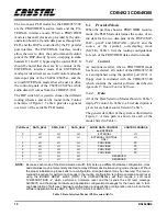
6. CLOCKING
There are four major clocks routed across the
CDB4923/300: CLKIN for the DSP, MCLK, LR-
CLK, and SCLK. CLKIN is only used to drive the
digital logic of the DSP core. MCLK, LRCLK, and
SCLK are used for synchronizing the audio sys-
tems of the CDB4923/300.
6.1
DSP Clock
The DSP clock of the CS492x/CS493xx is provid-
ed at the CLKIN pin (pin 30). The setting of jumper
J1 (DSP CLOCK) determines whether the
CS492x/CS493xx uses the input clock as the DSP
clock directly (CLKIN position) or uses the input
clock as a reference for the internal PLL (PLL po-
sition).
There are two possible clock sources on the
CDB4923/300. The first is the OSCILLATOR
(Y1). The second option is the external PLL (U26)
which can be configured to provide a processor
clock ranging from 33 MHz to 81 MHz. All clock-
ing circuitry can be found in Figure 8.
Since the PLL (U26) and the OSCILLATOR (Y1)
are co-dependent, only one can be used at any giv-
en time. Jumper J37 is used to select the source of
the main DSP clock. It is vital to note that the jump-
er J37 is a double jumper with two jumpers which
must be moved in unison. If the jumpers are not
moved together, board behavior will be unpredict-
able. Table 11 lists the oscillator requirements, and
the two different settings for J37, where pins 3 and
4 are connected to the inputs of the PLD. Jumper
J37 can also be found in Figure 8.
In order to use the 27 MHz oscillator directly, Y1
should be populated with the 27 MHz oscillator in-
cluded with the CDB4923/300 package. Addition-
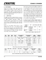
PLD
Mode
DATA
SEL2
DATA
SEL1
DATA
SEL0
CS492X/CS493XX
CMPDAT
CS492X/CS493XX
SDATAN1
MCLK
MASTER
CONTROL
SOURCE
0
LO
LO
LO
Data and Control lines accessed via J11 and J12
J12 or DSP
J11 & J12
1
LO
LO
HI
S/PDIF -- CS8414
A/D -- CS5334
CS8414
J11 & J12
2
LO
HI
LO
PC
A/D -- CS5334
DSP
PC
3
LO
HI
HI
S/PDIF -- CS8414
S/PDIF -- CS8414
CS8414
PC
4
HI
LO
LO
S/PDIF -- CS8414
A/D -- CS5334
CS8414
PC
5
HI
LO
HI
A/D -- CS5334
A/D -- CS5334
OSC/PLL
PC
6
HI
HI
LO
RESERVED
7
HI
HI
HI
RESERVED
Table 9. Data Selection Modes (Switch S3, PLD Version AB-X)
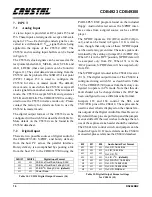
PLD
Mode
DATA_SEL2
DATA_SEL1
DATA_SEL0
CS492x/CS493xx
CMPDAT
CS492x/CS493xx
SDATAN1
MCLK
SOURCE
0
LO
LO
LO
J12
J12
J12 or DSP
1
HI
HI
HI
S/PDIF — CS8414
A/D -- CS5334
CS8414
Table 10. EXTERNAL Data Selection Modes (PLD Version AB-X)
Clock
Source
Y1
J37 - Pin 3 J37 - Pin 4
Oscillator
27 MHz or
12.288 MHz
oscillator
OSC
OSC
External
PLL
27 MHz
oscillator
PLL
PLL
Table 11. Board Clocking Configurations (J37)
Summary of Contents for CS492 Series
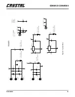
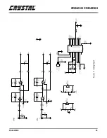
Page 18: ...CDB4923 CDB49300 18 DS262DB2 9 APPENDIX A SCHEMATICS Figure 4 CS492x CS493xx ...
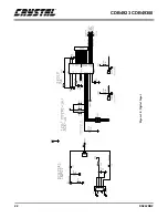
Page 19: ...CDB4923 CDB49300 DS262DB2 19 Figure 5 System Power ...
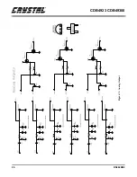
Page 20: ...CDB4923 CDB49300 20 DS262DB2 Figure 6 PC Interface ...
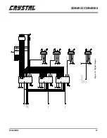
Page 21: ...CDB4923 CDB49300 DS262DB2 21 Figure 7 Control Logic ...
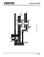
Page 22: ...CDB4923 CDB49300 22 DS262DB2 Figure 8 Clocking ...
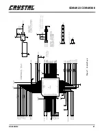
Page 23: ...CDB4923 CDB49300 DS262DB2 23 Figure 9 Analog Input ...
Page 24: ...CDB4923 CDB49300 24 DS262DB2 Figure 10 Digital Input ...
Page 25: ...CDB4923 CDB49300 DS262DB2 25 Figure 11 D A Converters ...
Page 26: ...CDB4923 CDB49300 26 DS262DB2 Figure 12 Analog Output ...
Page 27: ...CDB4923 CDB49300 DS262DB2 27 Figure 13 Digital Output ...
Page 28: ...CDB4923 CDB49300 28 DS262DB2 Figure 14 Top Layer ...
Page 29: ...CDB4923 CDB49300 DS262DB2 29 Figure 15 Bottom Layer ...
Page 30: ...CDB4923 CDB49300 30 DS262DB2 Figure 16 SSTOP ...
Page 31: ...CDB4923 CDB49300 DS262DB2 31 Figure 17 ASYSTOP ...
Page 32: ...CDB4923 CDB49300 32 DS262DB2 Figure 18 Layer 2 ...
Page 33: ...CDB4923 CDB49300 DS262DB2 33 Figure 19 Layer 3 ...
Page 49: ... Notes ...
Page 50: ......


