DS726PP2
19
CS4525
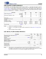
ANALOG INPUT CHARACTERISTICS
Test Conditions (unless otherwise specified): AGND = DGND = PGND = 0 V; All voltages with respect to ground;
T
A
= 25°C; VD = 3.3 V; Input Signal: 1 kHz sine wave through the recommended passive input filter shown in
; Capacitor values connected to AFILTA, AFILTB, FILT+, VQ, VD_REG, and VA_REG as shown
in
; Sample Frequency = 48 kHz; 10 Hz to 20 kHz Measurement Bandwidth; Power outputs in
power-down state (PDnOut1 = 1, PDnOut2 = 1, PDnOut3/4 = 1).
Notes:
4.
Referred to the typical full-scale voltage
5.
For VD = 2.5 V, VA_REG and VD_REG must be connected to VD. See
details.
6.
Measured between AINx and AGND.
ADC DIGITAL FILTER CHARACTERISTICS
Notes:
7.
Filter response is clock dependent and scales with the ADC sampling frequency (Fs). With a
27.000 MHz or 24.576 MHz XTAL/SYS_CLK, Fs is equal to the applied clock divided by 512. With an
18.432 MHz XTAL/SYS_CLK, Fs is equal to the applied clock divided by 384.
Parameter
Min
Typ
Max
Unit
Dynamic Range
A-weighted
unweighted
90
87
95
92
-
-
dB
dB
Total Harmonic Dist Noise
-1 dB
-20 dB
-60 dB
-
-
-
-86
-72
-32
-77
-
-
dB
dB
dB
DC Accuracy
Interchannel Gain Mismatch
-
0.05
-
dB
Gain Drift
-
±100
-
ppm/°C
Interchannel Isolation
-
90
-
dB
Full-scale Input Voltage
VD = 2.5V
VD = 3.3V
VD = 5.0V
0.786*VD
0.590*VD
0.398*VD
0.827*VD
0.621*VD
0.419*VD
0.868*VD
0.652*VD
0.440*VD
Vpp
Vpp
Vpp
Input Impedance
40
-
-
k
Ω
Parameter
Min
Typ
Max
Unit
Passband (Frequency Response)
to -0.1 dB corner
0
-
0.4948
Fs
Passband Ripple
-0.09
-
0
dB
Stopband
0.6677
-
-
Fs
Stopband Attenuation
48.4
-
-
dB
Total Group Delay
-
2.7/Fs
-
s
High-Pass Filter Characteristics
Frequency Response
-3.0 dB
-0.13 dB
-
-
3.7
24.2
-
-
Hz
Hz
Phase Deviation
20 Hz
-
10
-
Deg
Passband Ripple
-
-
0.17
dB
Filter Settling Time
-
10
5
/Fs
-
s

