background image

— 12 —

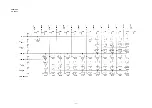
S T E P

O P E R A T I O N

D I S P L A Y

N O T E

Memory
Check

2

MEMORY

1  WR 1
2  READ 1

1

RAM WRITE 1

Write the test pattern 1 into RAM

MEMORY

1  WR 1
2  READ 1

After 1 sec.

2

EXECUTING !!

Read the test pattern 1 from RAM

CMPLETE !!

32/64/128 KB

After 1 sec.

Memory
Check

OK

MEMORY

1  WR 1
2  READ 1

3

RAM WRITE 2

Write the test pattern 2 into RAM

MEMORY

1  WR 1
2  READ 1

After 1 sec.

4

EXECUTING !!

Read the test pattern 2 from RAM

CMPLETE !!

32/64/128 KB

After 1 sec.

OK

MEMORY

1  WR 1
2  READ 1

5

XXXX

Wiring check for ROM

Memory
Check

OK

MEMORY

1  WR 1
2  READ 1

6

CHECK SUM
     TY     SZ     SUM     XOR
C5 0       512    XXX       XX

Check SUM value
     Version-  

E = 65D6

     Version-  

F = E146

OK

MEMORY

1  WR 1
2  READ 1

ESC

TEST
1  DISP
2  MEMORY
3  KEY

3  WR 2
4  READ 2
5  DUMP
6  CHKSUM

3  WR 2
4  READ 2
5  DUMP
6  CHKSUM

3  WR 2
4  READ 2
5  DUMP
6  CHKSUM

3  WR 2
4  READ 2
5  DUMP
6  CHKSUM

3  WR 2
4  READ 2
5  DUMP
6  CHKSUM

3  WR 2
4  READ 2
5  DUMP
6  CHKSUM

3  WR 2
4  READ 2
5  DUMP
6  CHKSUM
4  BUZZER
5  I/F
6  CONT
7  RESET

Summary of Contents for CSF-4450

Page 1: ...rice OCT 1995 CSF 4450 4650 4950 ZX 855 E F Version E and F Caution CSF 4 50 includes 2 kinds of version E and version F The functions are exactly the same between two versions As for details refer to page 1 INDEX ...

Page 2: ...FEATURES 1 SPECIFICATIONS 2 GENERAL GUIDE 5 BATTERY REPLACEMENT 6 RESET OPERATION 7 TO SAVE THE DATA 9 PIN FUNCTION 10 DIAGNOSTIC PROGRAM 11 ERROR MESSAGE 14 SCHEMATIC DIAGRAMS 15 EXPLODED VIEW 23 PARTS LIST 24 ...

Page 3: ... is different between two versions the functions are exactly the same A difference of two versions E and F cannot be confirmed from the appearance but it is recognized by production number on back of the backup battery cover as shown below VERSION TABLE FEATURES 3 color display The display shows data in three colors orange blue and green Different colors can be used to highlight specific dates in ...

Page 4: ... to model The following shows the memory capacity for each available model Model Memory CSF 4450 32K bytes 27 337 bytes CSF 4650 64K bytes 60 105 bytes CSF 4950 128K bytes 125 641 bytes The following shows the number or items that can be stored in each model CSF 4450 4650 4950 Telephone Directory Approximately 1 200 2 700 5 700 under the following conditions 8 character name 10 character telephone...

Page 5: ...Memo Schedule Keeper To Do Expense Manager Reminder Calendar Home Time World Time and Calculator Data storage Storage and recall of telephone business card memo schedule to do expense reminder data calendar display secret drawer editing memory status display Clock Worldtime reminder alarm schedule alarm to do alarm daily alarm accuracy under normal tempera tures 3 seconds average Calculation 12 di...

Page 6: ...tely 150 hours on type LR03 AM4 Back up 5 years if main batteries are replaced as soon as they become weak 2 year if dead main batteries are left in the unit Power consumption 0 06 W Auto power off Approximately 6 minutes after last key operation Operating temperature 0 C 40 C 32 F 104 F Dimensions Unfolded 10 5H 145W 176 5D mm 7 16 H 511 16 W 615 16 D Folded 14 2H 145W 95D mm 9 16 W 511 16 W 33 4...

Page 7: ... flashing 2 After selecting an icon press OK to access the functions of that icon Selecting some icons like the Clock and Telephone cause another selection screen to appear Details on actually using the features and functions that you access from the desktop are described in the other sections of this manual Changing the Desktop Screen s Window Scenery You can change the scenery that is outside th...

Page 8: ...er you finish adjusting the display contrast press OK Color contrast settings are registered as soon as you make them Because of this pressing either OK or ESC quits the color contrast procedure only Pressing ESC does not return the color contrast setting to what is was Notes Temperature changes can cause changes in background color and the tint of display colors Low battery power can also cause f...

Page 9: ...ove the cover 3 Insert a thin pointed object into A and remove the old battery RESET OPERATION 1 Press ON to switch power ON 2 Press the RESET button with a thin pointed object Warning The next step deletes all data stored in the CSF Unit s memory Make sure that you really want to delete the data before you continue 3 Remove both old batteries and replace them with two new ones Make sure that the ...

Page 10: ...C Daily Alarm 12 00 PM Sound Data alarm Schedule alarm Reminder alarm and To Do alarm ON Daily alarm OFF Key ON Messages English Character input CAPS To perform SECRET RESET Important The following procedure erases all data stored in the secret drawer Make sure you do not need any of the data in the secret drawer before deleting it You can transfer data you might need to the desktop page 9 before ...

Page 11: ... s unit MENU FUNC 2 1 3 OK If you can not succeed to transfer the data press ESC key on both units and try to transfer the data again following the procedure above TO STOP PRESS ESC DATA RECEIVE OK TO SAVE THE DATA CSF 4450 4650 4950 can transfer the customer s data to another CSF unit with memory protection only when replacing the LCD or the outer case To connect the CSF Unit to another CSF Unit ...

Page 12: ...1MHz clock input 83 PO O 1MHz clock output 84 VDD I 3V source 85 XO O 4 3MHz clock output 86 XI I 4 3MHz clock input 87 VCC I 3V source 88 VREG2 O Voltage for main switch detection 89 90 TS1 TS2 Test terminals of factory purpose only 91 VSSR I GND 92 BZZ1 O Buzzer signal output 93 BZZ2 O Buzzer signal output 94 VSS I GND 95 OCLK O Clock output 96 ITOFF I Switching terminal from main switch 97 TEMU...

Page 13: ...Blue color is displayed OK Checkers are displayed OK Reverse checkers are displayed OK Frame is displayed OK Dots at the 4 corners are displayed OK Vertical 4 colors are displayed OK Horizontal 4 colors are displayed OK TEST 1 DISP 2 MEMORY 3 KEY 4 BUZZER 5 I F 6 CONT 7 RESET 4 BUZZER 5 I F 6 CONT 7 RESET DIAGNOSTIC PROGRAM To enter the diagnostic program proceed as follows 1 Open the battery cove...

Page 14: ...UTING Read the test pattern 2 from RAM CMPLETE 32 64 128 KB After 1 sec OK MEMORY 1 WR 1 2 READ 1 5 XXXX Wiring check for ROM Memory Check OK MEMORY 1 WR 1 2 READ 1 6 CHECK SUM TY SZ SUM XOR C5 0 512 XXX XX Check SUM value Version E 65D6 Version F E146 OK MEMORY 1 WR 1 2 READ 1 ESC TEST 1 DISP 2 MEMORY 3 KEY 3 WR 2 4 READ 2 5 DUMP 6 CHKSUM 3 WR 2 4 READ 2 5 DUMP 6 CHKSUM 3 WR 2 4 READ 2 5 DUMP 6 C...

Page 15: ... bit N Non E Even or O Odd Key 7 BPS 9 9600 or 4 4800 1 EXECUTING Send the code H 2 No display Display the received charactor 3 EXECUTING Send the ASCII code 4 EXECUTING Loop back check ESC I F 7N9 CONTRAST ADJ 6 TEST 1 DISP 2 MEMORY 3 KEY Contrast up or SHIFT Contrast down or SHIFT CONTRAST O B G ORG BLU GRN Contrast adjustment Cursor keys CONTRAST O B G ORG BLU GRN Adjust the color using cursor ...

Page 16: ...ory area data item is sounding Attempt to enter the secret memory area using a password that does not match the one preset for the secret area Error during data communications Data communication has been interrupted Attempt to store a label that is identical to one already stored This message appears when this is the first time you ever turned on the CSF Unit Data corrupted by strong impact electr...

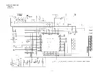
Page 17: ... 15 SCHEMATIC DIAGRAMS VERSION E Main Block 1 2 ...

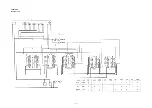
Page 18: ... 16 VERSION E Main Block 2 2 ...

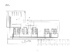
Page 19: ... 17 VERSION E Display Block ...

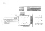
Page 20: ... 18 VERSION E Key Matrix ...

Page 21: ... 19 VERSION F Main Block 1 2 ...

Page 22: ... 20 VERSION F Main Block 2 2 ...

Page 23: ... 21 VERSION F Display Block ...

Page 24: ... 22 VERSION F Key Matrix ...

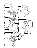
Page 25: ... 23 3 4 5 6 1 2 8 10 11 13 14 15 16 17 18 19 29 7 21 30 9 11 22 12 31 23 24 25 26 27 28 13 31 Version E Version F 20 7 12 EXPLODED VIEW ...

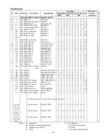
Page 26: ...4 MOS IC RH5VL23CA T1 1 1 1 1 1 1 1 1 1 1 10 B IC8 2105 4144 MOS IC RH5VL26CA T1 1 1 1 1 1 1 1 1 1 1 10 B N IC9 2105 5222 CMOS IC TC74HC04AF EL 1 1 1 1 1 1 1 1 1 1 10 B L1 3841 1799 Coil 636CY 151M P3 1 1 1 1 1 1 1 1 1 1 5 C LSI2 6413 5320 COF3011 F1 SUB A340214 1 0 1 0 0 1 1 0 1 0 1 1 B ASS Y N LSI3 2012 2394 LSI UPD23C4001EJGW C17 0 1 0 0 1 1 0 1 0 1 B N LSI3 2012 3493 LSI UPD23C4001EJGW C31 1 0...

Page 27: ...1 1 1 1 1 1 1 R19 Chip Resistor MCR03EZHG392 1 1 1 1 1 1 1 1 1 1 R20 Chip Resistor MCR03EZHF1053 0 1 0 0 1 1 0 1 0 1 R20 Chip Resistor MCR03EZHF4532 1 0 1 1 0 0 1 0 1 0 R21 R32 Chip Resistor MCR03EZHJ000 0 2 0 0 0 0 0 2 0 2 R21 R32 Chip Resistor MCR03EZHJ000 7 0 0 0 0 0 7 0 7 0 R42 R100 R106 R111 R208 R21 R74 Chip Resistor MCR03EZHJ000 0 0 0 0 2 2 0 0 0 0 R21 R74 Chip Resistor MCR03EZHJ000 0 0 7 7...

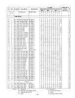
Page 28: ...6417 2160 Lower Case Z855A MC100006 1 1 1 0 0 0 0 0 0 0 0 5 X N 15 6417 2330 Lower Case Z855E MC100006 2 0 0 1 0 1 0 0 0 0 0 5 X N 15 6417 2400 Lower Case Z855F MC100006 3 0 0 0 1 0 1 0 0 0 0 5 X N 15 6417 2440 Lower Case Z855I MC100006 4 0 0 0 0 0 0 1 1 0 0 5 X N 15 6417 2520 Lower Case Z855J MC100006 5 0 0 0 0 0 0 0 0 1 1 5 X N 16 6417 2190 B Cover B Z855A MC300501 1 1 1 0 0 0 0 0 0 0 0 20 C N 1...

Page 29: ...2460 B Cover A Z855I MC300500 3 0 0 0 0 0 0 1 1 1 1 20 C 28 6416 5860 Badge Label Z850 C440972 1 1 1 1 1 1 1 1 1 1 1 20 X 31 6408 9410 Battery Spring B C311911 2 1 1 1 1 1 1 1 1 1 1 20 C LCD ASS Y N LSI10 6417 3871 OC3015 F1 SUB C340532 3 1 0 1 1 0 0 1 0 1 0 1 B ASS Y N 7 3335 6055 LCD CD1034 TS 1 0 1 1 0 0 1 0 1 0 1 B N 30 5610 9170 Heat Seal Z855 MC300502 1 1 0 1 1 0 0 1 0 1 0 1 B Notes N New pa...

Page 30: ...8 11 10 Nishi Shinjuku Shinjuku ku Tokyo 160 Japan Telephone 03 3347 4926 ...

Reviews: