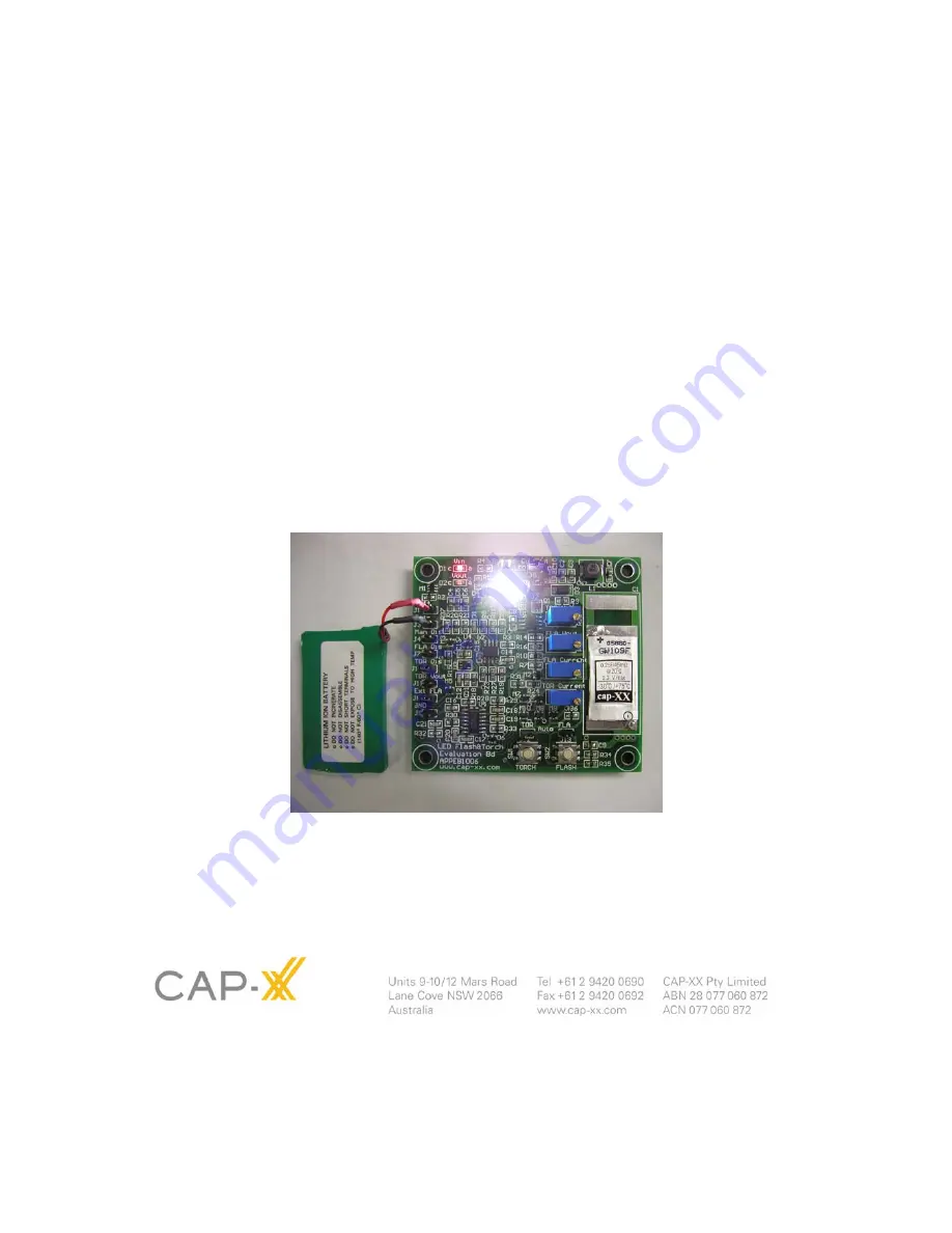
User’s Manual
Camera Phone Flash
Evaluation Board
APPEB1006
All information contained herein is strictly confidential
APPEB1006 User Manual rev1.0, 31-May-2005 page 1 of 6
© CAP-XX Pty Limited 2005
Page 1: ...User s Manual Camera Phone Flash Evaluation Board APPEB1006 All information contained herein is strictly confidential APPEB1006 User Manual rev1 0 31 May 2005 page 1 of 6 CAP XX Pty Limited 2005 ...
Page 2: ...ll retrigger approximately every 2 5s This duty cycle is imposed due to the thermal constraints of the white LED Circuit Description refer to schematics at the end of this manual Input Voltage The circuit is designed to operate from an external Li ion battery 4 2V 3 3V Vbat is the node connected to the battery via J1 J1 is to be connected to battery positive terminal Pins 1 and 2 of J1 are joined ...
Page 3: ... this voltage is increased not to overvoltage the supercap ie the supercap voltage will be Vout minus the voltage of the battery For maximum supercapacitor life the voltage should be kept below 2 3V however short term overvoltages seconds may go up to 2 7V TORCH MODE The continuous current required for TORCH is FLASH current typically 100mA Vs 1A Therefore the voltage dropped across the LED will b...
Page 4: ...orch Mode Control If J12 is jumpered then Torch mode will be permanently on Auto Torch Alternatively an external control signal connected to pin 2 of J12 will select Torch mode when Hi 3V 5V This logic signal drives the gates of M8 M9 and M10 and must source 0 1mA to develop 3 3V across R36 Flash PulseTimers External Flash Pulse Control There are two on board 555 timers One generates the FLASH on ...
Page 5: ...e FB GND Vdrive Vin C3 10u 805 R14 1k 805 Boost Disable 3V 1V2 3V R11 47k 805 C11 10u 805 C18 100n 805 D2 LYR976 805 J2 Inductor Current 1 2 R37 150 805 R10 100k 805 R1 82k 805 R8 18k 805 R17 T93YB 2k 3 1 2 R28 220k 805 C7 10u 805 R30 33k 805 3V U5 TLC556CD SOIC 1 2 3 4 5 6 7 8 9 10 11 12 13 14 DIS TH CON RES OUT TRIG GND TRIG OUT RES CON TH DIS VCC Vbat Offtime Trigger Undervoltage Lockout Vmin 3...
Page 6: ...dd M7 FDV301N M5 FDV301N J8 External Timer 1 2 R24 33k 805 Offtime Trigger R26 T93YB 2k 3 1 2 3V C15 220p 603 R20 33k 805 J7 Pulse Boost Disable 1 2 Boost Disable R19 100k 805 1V2 R36 33k 805 J10 Torch Boost Disable 1 2 SW1 Torch B3SN M4 ZXM64NO2X MSOP8 1 4 5 7 8 6 2 3 R22 R047 805 3V 3V M8 FDV301N R31 33k 805 Boost Disable M6 FDV301N Pulse R23 3k3 805 3V Torch Flash J9 GND 1 2 D5 LumiLED M10 FDV3...