11
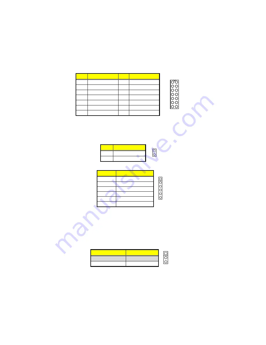
CN10/CN12: LVDS Interface Connector
PIN Description PIN Description
1
V
LCD
2
V
LCD
3
GND
4
GND
5
A0-/B0-
6
A0+/B0+
7
A1-/B1-
8
A1+/B1+
9
A2-/B2-
10
A2+/B2+
11
CLK1-/CLK2-
12
CLK1+/CLK2+
13
A3-/B3-
14
A3+/B3+
1
2
13
14
NOTE:
LVDS cable should be produced very carefully. A0- & A0+ have to
be fabricated in twister pair (A1- & A1+, A2- & A2+ and so on)
otherwise the signal won’t be stable. Please set the proper voltage
of your panel using JP1 before proceeding on installing it.
CN30: DVI SM Bus
PIN Description
1
SPD1
2
SPCLK1
2
1
CN7: Inverter Power Connector
PIN
Description
1
+12V
2
+12V
3
VCC
4
BK_EN
5
ENVDD
6
GND
1
6
NOTE:
If use CN10 only, it just supports 24-bit single channel LVDS
panel; If you want to use 48-bit dual channel LVDS panel, please
use CN10 and CN12 combined.
The HS-2613 has an onboard jumper that selects the working voltage
of the flat panel connected to the system. Jumper
JP1
offers two
voltage settings for the user.
JP1: Panel Voltage Select
Options
Settings
+3.3V (default)
Short 1-2
+5V
Short 2-3
1
3
Summary of Contents for HS-2613
Page 14: ...8 3 2 Board Layout...
Page 34: ...28 This page is the blank page...
Page 50: ...44 This page is the blank page...


