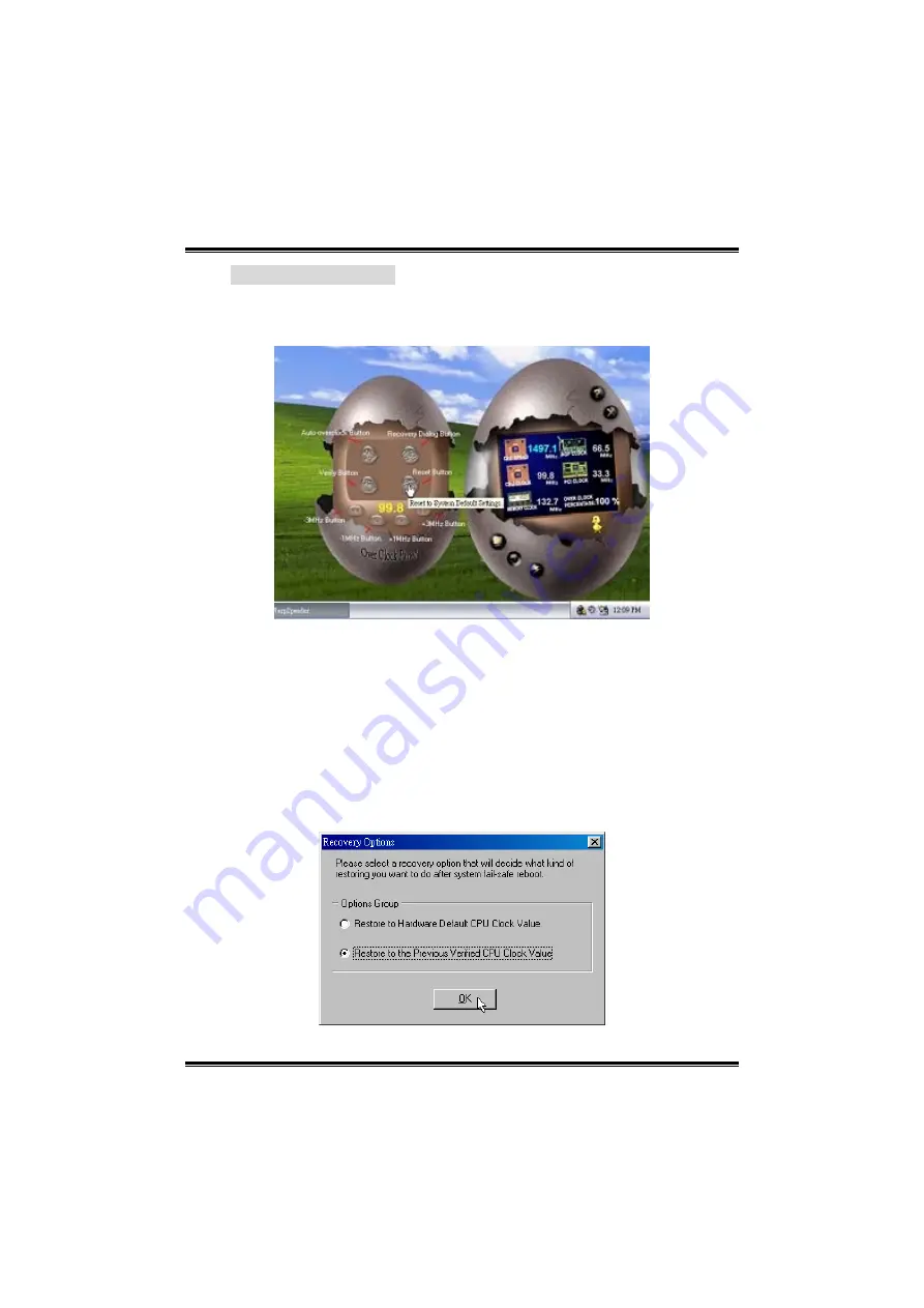
Biostar GeForce 6100 M7 User Manual Download Page 26

GeForce 6100-M7 

24 

4.  Overclock Panel 

Click the Overclock button in Main Panel, the button will be 
highlighted and the Overclock Panel will slide out to left as the 
following figure. 


Overclock Panel contains the these features:   

a.  “–3MHz button”, “-1MHz button”, “+1MHz button”, and “+3MHz button”: 

provide user the ability to do real-time overclock adjustment. 

Warning:  

Manually overclock is potentially dangerous, especially when the 
overclocking percentage is over 110 %. We strongly recommend you 
verify every speed you overclock by click the Verify button. Or, you can 
just click Auto overclock button and let [WarpSpeeder™] automatically 
gets the best result for you. 

b.  “Recovery Dialog button”: Pop up the following dialog. Let user select 

a restoring way if system need to do a fail-safe reboot. 


Summary of Contents for GeForce 6100 M7

Page 1: ...will not occur in a particular installation The vendor makes no representations or warranties with respect to the contents here and specially disclaims any implied warranties of merchantability or fit...

Page 2: ...rs 6 2 3 Installing System Memory 7 2 4 Connectors and Slots 8 Chapter 3 Headers Jumpers Setup 10 3 1 How to Setup Jumpers 10 3 2 Detail Settings 10 Chapter 4 Useful Help 16 4 1 Award BIOS Beep Code 1...

Page 3: ...cm W Operating System Supporting Supports Windows 2000 and Windows XP Note Does not support Windows 98SE and Windows ME Slot Two PCI bus master slots One PCI E x1 slot One PCI E x16 slot On board IDE...

Page 4: ...c Chip ALC655 Support 6 channels Supports S PDIF out function Compliant with AC 97 Version 2 3 specification Onboard Serial ATA Integrated in nForce 410 Four serial ATA connectors support 2 SATA devic...

Page 5: ...or supports 2 Floppy drives with 360K 720K 1 2M 1 44M and 2 88Mbytes 2 IDE connectors support 4 hard disk devices 2 Serial ATA connectors support 2 SATA devices 2 USB headers support 4 USB 2 0 ports a...

Page 6: ...O1 JUSBLAN1 BIOS PCI EX1_1 PCI EX16 PCI1 FDD1 BAT1 JCOM1 JUSBV1 JCDIN1 Codec LAN PHY JFAUDIO1 JATXPWR2 JSPDIF_OUT1 PCI2 Super I O JUSBV2 JUSB2 JUSB3 DIMM2 DIMM1 JSFAN1 JCI1 JCMOS1 JPANEL1 IDE1 IDE2 JA...

Page 7: ...e angle 90 A Step 2 Look for the black triangle on socket and the white triangle on CPU should point forwards this black triangle The CPU will fit only in the correct orientation Step 3 Hold the CPU d...

Page 8: ...nnector while matching the black wire to pin 1 JCFAN1 CPU Fan Header JSFAN1 System Fan Header Pin Assignment 1 Ground 2 12V JSFAN1 3 1 1 3 JCFAN1 3 FAN RPM rate sense Note The JCFAN1 and JSFAN1 suppor...

Page 9: ...e slot such that the notch on the DIMM matches the break on the Slot 2 Insert the DIMM vertically and firmly into the slot until the retaining chip snap back in place and the DIMM is properly seated N...

Page 10: ...rive ribbon cables 34 33 1 2 IDE1 IDE2 Hard Disk Connectors The motherboard has a 32 bit Enhanced PCI IDE Controller that provides PIO Mode 0 4 Bus Master and Ultra DMA 33 66 100 133 functionality It...

Page 11: ...l Component Interconnect and it is a bus standard for expansion cards This PCI slot is designated as 32 bits PCI2 PCI1 PCI EX16 PCI Express x16 Slot PCI Express 1 0a compliant Maximum bandwidth is up...

Page 12: ...ers for USB Ports Pin 1 2 Close JUSBV1 5V for USB ports at JUSB1 and JUSBLAN1 JUSBV2 5V for USB ports at front panel JUSB2 JUSB3 Pin 2 3 Close JUSBV1 USB ports at JUSB1 and JUSBLAN1 are powered by 5V...

Page 13: ...2 3 3V 3 Ground 4 5V 5 Ground 6 5V 7 Ground 8 PW_OK 9 Standby Voltage 5V 10 12V 11 12V 12 3 3V 13 3 3V 14 12V 15 Ground 16 PS_ON 17 Ground 18 Ground 19 Ground 20 5V 21 5V 22 5V 23 5V 12 24 1 13 24 Gro...

Page 14: ...5 USB 6 USB 7 Ground 8 Ground 9 Key 1 2 9 10 JUSB3 JUSB2 10 NC JCDIN1 CD ROM Audio in Connector This connector allows user to connect the audio source from the variaty devices like CD ROM DVD ROM PCI...

Page 15: ...peaker out Right 6 Right line out Speaker out Right 7 Reserved 8 Key 9 Left line out Speaker out Left 10 Left line out Speaker out Left 11 Right line in optional 12 Right line in optional 13 Left line...

Page 16: ...Pin 2 3 Close Clear CMOS data Clear CMOS Procedures 1 Remove AC power line 2 Set the jumper to Pin 2 3 close 3 Wait for five seconds 4 Set the jumper to Pin 1 2 close 5 Power on the AC 6 Reset your de...

Page 17: ...PWR_LED On Off IR IR RST HLED SPK 2 Pin Assignment Function Pin Assignment Function 1 5V 2 Sleep control 3 N A 4 Ground Sleep button 5 N A 6 N A N A 7 Speaker Speaker Connector 8 Power LED 9 HDD LED 1...

Page 18: ...e BIOS If the following message is shown after boot up the system it means the BIOS contents are corrupted In this Case please follow the procedure below to restore the BIOS 1 Make a bootable floppy d...

Page 19: ...again In this case please double check 1 The CPU cooler surface is placed evenly with the CPU surface 2 CPU fan is rotated normally 3 CPU fan speed is fulfilling with the CPU speed After confirmed ple...

Page 20: ...o disk controller board Make sure both ends are securely plugged in check the drive type in the standard CMOS setup 2 Backing up the hard drive is extremely important All hard disks are capable of bre...

Page 21: ...nformation Also in the About panel you can get detail descriptions about BIOS model and chipsets In addition the frequency status of CPU memory AGP and PCI along with the CPU speed are synchronically...

Page 22: ...he following dialog in setup procedure it means setup is completed If the Launch the WarpSpeeder Tray Utility checkbox is checked the Tray Icon utility and WarpSpeeder utility will be automatically an...

Page 23: ...responsible for conveniently invoking WarpSpeeder Utility You can use the mouse by clicking the left button in order to invoke WarpSpeeder directly from the little tray icon or you can right click the...

Page 24: ...lows a Display the CPU Speed CPU external clock Memory clock AGP clock and PCI clock information b Contains About Voltage Overclock and Hardware Monitor Buttons for invoking respective panels c With a...

Page 25: ...l be highlighted and the Voltage Panel will slide out to up as the following figure In this panel you can decide to increase CPU core voltage and Memory voltage or not The default setting is No If you...

Page 26: ...de user the ability to do real time overclock adjustment Warning Manually overclock is potentially dangerous especially when the overclocking percentage is over 110 We strongly recommend you verify ev...

Page 27: ...y If the testing fail system will do a fail safe rebooting After reboot the WarpSpeeder utility will restore to the hardware default setting or load the verified best and stable frequency according to...

Page 28: ...highlighted and the About Panel will slide out to up as the following figure In this panel you can get model name and detail information in hints of all the chipset that are related to overclocking Y...

Page 29: ...es are controlled by several separate chipset WarpSpeeder divide these features to separate panels If one chipset is not on board the correlative button in Main panel will be disabled but will not int...

Reviews: