background image

SBC82621 Socket370 Half-size All-in-One CPU Card User’s Manual


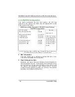
4.2.7  PC Health Status 

This section is to monitor the current hardware status of core 
voltages. This is available only if there is hardware monitoring 
mechanism onboard.  

CMOS Setup Utility-Copyright © 1984-2001 Award Software 

PC Health Status 

Current CPU Temp. 


Item Help 

Current System Temp. 


Current CPUFAN1 Speed 


Menu Level   

Vcore  


2.5V  


3.3V  


5V  


12V  


 : Move  Enter: Select  +/-/PU/PD: Value  F10: Save  ESC: Exit F1: General Help 

F5: Previous Values F6: Fail-Safe Defaults F7: Optimized Defaults 


Current CPU Temp. 

Show you the current CPU temperature.


Current System Temperature 

These read-only fields reflect the functions of the hardware 
thermal sensor that monitors the chip blocks and system 
temperatures to ensure the system is stable. 


Current CPUFAN1 Speed 

These optional and read-only fields show the current 
speeds in RPM (revolution per minute) for the CPU fan and 
chassis fan as monitored by the hardware monitoring IC.  

Award BIOS Utility 

53 

Summary of Contents for SBC82621

Page 1: ...SBC82621 Series Socket370 Half size All in One CPU Card User s Manual ...

Page 2: ...IOMTEK makes no commitment to update or to keep current the information contained in this manual AXIOMTEK reserves the right to make improvements to this document and or product at any time and without notice No part of this document may be reproduced stored in a retrieval system or transmitted in any form or by any means electronic mechanical photocopying recording or otherwise without the prior ...

Page 3: ...s when handling boards and components Trademarks Acknowledgments AXIOMTEK is a trademark of AXIOMTEK Co Ltd IBM is a registered trademark of International Business Machines Corporation MS DOS and Windows 95 98 NT 2000 XP ME are trademarks of Microsoft Corporation Award is a trademark of Award Software Inc IBM PC AT PS 2 VGA are trademarks of International Business Machines Corporation Intel Pentiu...

Page 4: ...This page does not contain any information iv ...

Page 5: ...l Connector VDDM of CN1 JP1 8 2 3 4 COM RS232 422 485 Setttings JP2 JP4 JP5 8 2 3 5 DiskOnChip Memory Segment JP6 9 2 3 6 USB Wake Up Settings JP7 9 2 4 Connectors 10 2 4 1 VGA Interface 11 2 4 2 Floppy Disk Controller 18 2 4 3 Parallel Port Interface 18 2 4 4 Serial Port Interface 19 2 4 5 Real Time Clock and CMOS RAM 19 2 4 6 Keyboard and Mouse Connectors 19 2 4 7 USB Connector 20 2 4 8 IrDA Con...

Page 6: ...er 4 Award BIOS Utility 29 4 1 BIOS Introduction 29 4 2 BIOS Setup 29 4 2 1 Standard CMOS Setup 31 4 2 2 Advanced BIOS Features 35 4 2 3 Advanced Chipset Features 39 4 2 4 Integrated Peripherals 43 4 2 5 Power Management Setup 47 4 2 6 PNP PCI Configuration 50 4 2 7 PC Health Status 53 4 2 8 Frequency Voltage Control 54 4 2 9 Load Fail Safe Defaults 55 4 2 10 Load Optimized Defaults 56 4 2 11 Save...

Page 7: ...performance and function rich capability The CPU incorporates the VIA VT8606 chipset and the VT82C686B with built in AGP 4x VGA controller This combination ensures its compatibility with ISA bus passive backplanes Designed for the professional embedded developers the Socket370 all in one SBC82621 CPU card is virtually the ultimate one step solution to various applications Introduction 1 ...

Page 8: ...e 1 x PS 2 Keyboard Interface 1 x PS 2 Mouse Interface 1 x IrDA interface for wireless communication System Memory 1 x 168 pin DIMM socket Maximum of 512MB SDRAM ECC parity checking L2 Cache integrated in CPU Watchdog Timer Generates a system reset or NMI by jumper selectable Software programmable time interval 64 levels 0 5 8 5 80 50 800 100 1600 seconds Ethernet Dual Realtek 8100C PCI Bus 10 100...

Page 9: ...laced CRT monitors and 1024 x 768 16 bit color on LCD panel monitors USB Interface use a VIA VT6212 4 Port Host Controller support two ports USB Spec Rev 2 0 compliant DiskOnChip ports DisksupOnChip Expansion Slots one 16 bit PC 104 connector Dimensions 121 92 x 185 mm NOTE Specifications are subject to change without notice 1 3 Utilities Supported VIA Chipset Drivers Ethernet Utility Flat panel C...

Page 10: ...SBC82621 Socket370 Half size All in One CPU Card User s Manual This page does not contain any information Introduction 4 ...

Page 11: ...ze All in One CPU Card User s Manual C h a p t e r 2 Jumpers and Connectors 2 1 Jumpers and Connectors Layout The following figure shows the layout of all jumpers and connectors on the SBC82621 CPU card Jumpers and Connectors 5 ...

Page 12: ...Socket370 Half size All in One CPU Card User s Manual 2 2 Jumpers and Connectors Dimensions The following figure shows the location of all jumpers and connectors on the SBC82621 CPU card Jumpers and Connectors 6 ...

Page 13: ... Trigger Mode Disabled Open JP4 COM2 Port Setting RS 232 Short 3 5 4 6 JP5 COM2 Port Setting RS 232 Short 1 2 JP6 DiskOnChip Memory Segment D0000 D1FFF Short 1 2 JP7 USB Wake Up Selection Disabled Short 2 3 JP8 Clear CMOS Setting Normal Short 1 2 2 3 1 Watchdog Trigger Mode Setting JP3 The watchdog timer is an indispensable feature of the SBC82621 It has a sensitive error detection function and a ...

Page 14: ...lat panel displays When using such type of flat panels configure jumper JP1 to the appropriate voltage of the flat panel VDDM Settings 5V default Short 2 3 1 2 3 3 3V Short 1 2 2 3 4 COM RS232 422 485 Settings JP2 JP4 JP5 COM4 JP2 JP4 JP5 RS 232 default Short 3 5 4 6 Short 3 5 4 6 Short 1 2 RS 422 Short 1 3 2 4 Short 1 3 2 4 Short 3 4 RS 485 Short 1 3 2 4 Short 1 3 2 4 Short 5 6 7 8 JP2 and JP4 2 ...

Page 15: ...Chip Memory Segment JP6 Options Settings D0000 D1FFF default Short 1 2 D2000 D3FFF Short 3 4 D4000 D5FFF Short 5 6 2 4 6 1 3 5 7 8 D6000 D7FFF Short 7 8 2 3 6 USB Wake Up Settings JP7 Options Settings Enabled default Short 1 2 1 2 3 Disabled Short 2 3 Jumpers and Connectors 9 ...

Page 16: ...ch connector on the SBC82621 Connectors Label IDE Connector IDE1 FDD Connector FDD1 44 pin LCD Connector CN1 20 pin LCD Connector CN2 Flat Panel Bezel Connector CN3 Power Input Connectors CN4 CN8 PC104 Connector CN5 CN6 PS 2 Keyboard and Mouse Connector CN7 Keyboard Connector CN9 Mouse Connector CN10 ACPI Connector CN11 ATX PS_ON Switch CN12 Printer Port Connector PRT1 VGA Connector VGA1 IrDA Conn...

Page 17: ... up to 16M colors on 36 bit active matrix flat panels 2 4 1 2 Features Fully compatible with IBMTM VGA Flat panel and CRT monitor can be displayed simultaneously The VGA RAM support system main memory up to 64MB Supports panel resolution up to 1280x1024 Supports non interlaced CRT monitors with resolutions up to 1920x1440 24 bits colors Direct interface to Color and Monochrome Dual Drive and Singl...

Page 18: ...e the pin assignments for the CRT VGA connector and the flat panel connector VGA1 CRT VGA Connector Pin Assignment Pin Description Pin Description Pin Description 1 Red 2 Green 3 Blue 4 N A 5 GND 6 AGND 7 AGND 8 AGND 9 N A 10 GND 11 N A 12 DDC DAT 13 Horizontal Sync 14 Vertical Sync 15 DDC CLK CN1 Flat Panel Connector Pin Assignment Pin Description Pin Description Pin Description 1 12V 2 12VM 3 GN...

Page 19: ...nector Pin Description Name Description P0 P35 Flat panel data output ENABKL Activity Indicator and Enable Backlight outputs SHFCLK Shift clock Pixel clock for flat panel data M M signal for panel AC drive control LP Latch pulse Flat panel equivalent of HSYNC FLM First line marker Flat panel equivalent of VSYNC 12VM 12V power controlled by chipset ENAVEE ENAVDD Power sequencing controls for panel ...

Page 20: ... VSYNC VSYNC SHFCLK XCK XCK CK CK M DE DE DE DE ENAVDD ENAVDD ENAVDD ENAVDD ENAVDD ENABLK ENABLK ENABLK ENABLK ENABLK P0 R0 R0 R0 LR0 P1 G0 G0 G0 P2 B0 B0 B0 LG0 P3 R1 R1 R1 P4 G1 G1 G1 LB0 P5 B1 B1 B1 P6 R2 R2 R2 LR1 P7 G2 G2 G2 P8 B2 B2 P9 R3 R3 P10 G3 G3 P11 B3 B3 P12 R4 R4 P13 G4 G4 P14 B4 B4 P15 R5 R5 P 6 G5 P17 B5 P18 R6 UR0 P19 G6 P20 B6 UG0 P21 R7 P22 G7 UB0 P23 B7 P24 UR1 Jumpers and Conn...

Page 21: ...DD ENABLK ENABLK ENABLK ENABLK ENABLK P0 LB3 P1 LB2 P2 LB1 LB1 P3 LB0 LB0 P4 UB3 P5 UB2 P6 UB1 UB1 R0 R00 P7 UB0 UB0 R10 P8 LG3 R1 R01 P9 LG2 R11 P10 LG1 LG1 R2 R02 P11 LG0 LG0 R12 P12 UG3 P13 UG2 P14 UG1 UG1 P15 UG0 UG0 P 6 LR3 P17 LR2 P18 LR1 LR1 G0 G00 P19 LR0 LR0 G10 P20 UR3 G1 G01 P21 UR2 G11 P22 UR1 UR1 G2 G02 P23 UR0 UR0 G12 P30 B0 B00 P31 B10 P32 B1 B01 P33 B11 P34 B2 B02 P35 B12 Jumpers a...

Page 22: ...VDD ENAVDD ENAVDD ENAVDD ENABLK ENABLK ENABLK ENABLK ENABLK P0 P1 P2 R0 R00 P3 R10 P4 R0 R00 R1 R01 P5 R10 R11 P6 R1 R01 R2 R02 P7 R11 R12 P8 R2 R02 R3 R03 P9 R12 R13 P10 R3 R03 R4 R04 P11 R13 R14 P12 P13 P14 G0 G00 P15 G10 P 6 G0 G00 G1 G01 P17 G10 G11 P18 G1 G01 G2 G02 P19 G11 G12 P20 G2 G02 G3 G03 P21 G12 G13 P22 G3 G03 G4 G04 P23 G13 G14 P24 P25 P26 B0 B00 P27 B10 Jumpers and Connectors 16 ...

Page 23: ...TFT TFT Pin 18 bit 24 bit 2X18 bit LP LP LP HSYNC FLM FP FP VSYNC SHFCLK XCK XCK CK M DE DE DE ENAVDD ENAVDD ENAVDD ENAVDD ENABLK ENABLK ENABLK ENABLK P0 B0 R00 P1 B1 R10 P2 B0 B2 R01 P3 B1 B3 R11 P4 B2 B4 R02 P5 B3 B5 R12 P6 B4 B6 R03 P7 B5 B7 R13 P8 G0 R04 P9 G1 R14 P10 G0 G2 R05 P11 G1 G3 R15 P12 G2 G4 G00 P13 G3 G5 G10 P14 G4 G6 G01 P15 G5 G7 G11 P16 R0 G02 P17 R1 G12 P18 R0 R2 G03 P19 R1 R3 G...

Page 24: ...following types 5 25 360KB 1 2MB and 3 5 720KB 1 44MB 2 88MB The FDD1 pin assignment is listed in Appendix B 2 4 3 Parallel Port Interface The SBC82621 onboard PRT1 is a multi mode parallel port able to support Standard mode IBM PC XT PC AT and PS 2 compatible with bi directional parallel port Enhanced mode Enhance parallel port EPP compatible with EPP 1 7 and EPP 1 9 IEEE 1284 compliant High spee...

Page 25: ... for COM1 and COM2 along with the RS 485 pin assignments for COM2 are in Appendix B 2 4 5 Real Time Clock and CMOS RAM The SBC82621 contains VT82C686B Integrated Real Time Clock RTC and 128 bytes of CMOS RAM The CMOS RAM stores the system configuration information entered via the SETUP program A battery with power lasting 10 years keeps the stored information on the RTC and CMOS RAM active when sy...

Page 26: ...ial Bus USB connector on the SBC82621 is for installation of peripherals supporting the USB interface USB1 is the 10 pin USB connector on the SBC82621 USB1 9 10 1 2 USB Power USB P0 USB P0 USB GND AGND USB Power USB P1 USB P1 GND USB AGND 2 4 8 IrDA Connector IR1 is a 5 pin IrDA connector for wireless communication IR1 1 2 5 4 3 5V N C IRRX GND IRTX Jumpers and Connectors 20 ...

Page 27: ...n the table below Pin Description 1 12V 2 GND 3 GND 1 4 5V 2 4 10 ACPI Connector Advanced Configuration and Power Interface ACPI defines a flexible and extensible interface that allows system designers to select appropriate cost feature trade offs for power management The interface enables and supports reliable power management through improved hardware and operating system coordination The specif...

Page 28: ...sound module fax modem module and multi I O module etc CN5 PC 104 Bus Pin Assignment Pin Pin Name Pin Pin Name Pin Pin Name Pin Pin Name 1 IOCHCHK 2 GND 3 SD7 4 RESETDRV 5 SD6 6 5V 7 SD5 8 IRQ9 9 SD4 10 5V 11 SD3 12 DRQ2 13 SD2 14 12V 15 SD1 16 ENDXFR 17 SD0 18 12V 19 IOCHRDY 20 GND 21 AEN 22 SMEMW 23 SA19 24 SMEMR 25 SA18 26 IOW 27 SA17 28 IOR 29 SA16 30 DACK3 31 SA15 32 DRQ3 33 SA14 34 DACK1 35 ...

Page 29: ...A21 11 IRQ12 12 LA20 13 IRQ15 14 LA19 15 IRQ14 16 LA18 17 DACK0 18 LA17 19 DRQ0 20 MEMR 21 DACK5 22 MEMW 23 DRQ5 24 SD8 25 DACK6 26 SD9 27 DRQ6 28 SD10 29 DACK7 30 SD11 31 DRQ7 32 SD12 33 5V 34 SD13 35 MASTER 36 SD14 37 GND 38 SD15 39 GND 40 KEY 2 4 12 CPU Fan Connector FAN1 FAN2 Pin Description 1 GND 2 5V 1 2 3 3 SPEED SENSOR 2 4 13 Flat Panel Bezel Connector CN3 1 3 5 7 9 11 2 4 6 8 10 12 Jumper...

Page 30: ...ect to the case mounted reset switch and allow rebooting of your computer instead of turning OFF the power switch This is a preferred method of rebooting in order to prolong the life of the system s power supply HDD Activity LED This connector extends to the hard drive activity LED on the control panel This LED will flash when the HDD is being accessed Pins 10 12 of CN3 connect the hard disk drive...

Page 31: ... Bus speeds for 66M 100M and 133MHz The CPU Bus Clock is auto detected and generated by a clock generator 3 3 BIOS The system BIOS used in SBC82621 is Award Plug and Play BIOS The SBC82621 contains a single 4M bit Flash EPROM 3 4 System Memory The SBC82621 inductrial CPU board supports one 168 pin DIMM Dual In Line Memory Module socket for a maximum memory of 256MB buffer SDRAMs The memory module ...

Page 32: ...phics accelerator into a single chip TwisterT brings mainstream graphics performance to the Value PC with leading edge 2D 3D and DVD video acceleration into a cost effective package Based on its capabilities Twister T is an ideal solution for the consumer corporateration users and entry level professionals The industry s first integrated AGP 4X solution TwisterT combines AGP 4X performance with Mi...

Page 33: ...80 09F DMA page register 0A0 0BF Interrupt controller 2 0F0 Clear math coprocessor busy signal 0C0 0DF DMA controller 2 0F1 Reset math coprocessor 0F8 0FF Math processor 120 Disable watchdog timer operation read 121 Enable watchdog timer operation read 122 Watchdog 123 Board ID 1F0 1F8 Fixed disk controller 200 207 Game port 300 31F Prototype card 360 36F Reserved 378 37F Parallel port 1 3B0 3BF M...

Page 34: ...ist of the 16 interrupt request lines is shown below NMI Parity check error IRQ0 System timer output IRQ1 Keyboard IRQ2 Interrupt rerouting from IRQ8 through IRQ15 IRQ3 Serial port 2 IRQ4 Serial port 1 IRQ5 Reserved IRQ6 Floppy disk controller IRQ7 Parallel port 1 IRQ8 Real time clock IRQ9 Reserved IRQ10 Reserved IRQ11 USB IRQ12 PS 2 Mouse IRQ13 Math coprocessor IRQ14 Primary IDE channel IRQ15 Sec...

Page 35: ...tem 4 2 BIOS Setup The Award BIOS provides a Setup utility program for specifying the system configurations and settings The BIOS ROM of the system stores the Setup utility When you turn ON the computer the Award BIOS is immediately activated Pressing the Del key immediately allows you to enter the Setup utility If you are a little bit late pressing the Del key POST Power On Self Test will continu...

Page 36: ...enu in BIOS Select Item F10 Save Exit Setup F6 SAVE CMOS TO BIOS F7 LOAD CMOS FROM BIOS Time Date Hard Disk Type The section below the setup items of the Main Menu displays the control keys for this menu Another section located at the bottom of the Main Menu just below the control keys section displays information on the currently highlighted item in the list NOTE If you find that your computer ca...

Page 37: ...Primary Master Press Enter None IDE Primary Slave Press Enter None Press Enter to enter next page for detail Drive A 1 44M 3 5 in hard drive settings Drive B None LCD Type T1 1024x768 DSTN CRT Screen Expansion Enabled Display Type During POST Default Display Type After POST Default Halt On All But Keyboard Base Memory 640K Extended Memory 65472K Total Memory 1024K Move Enter Select PU PD Value F10...

Page 38: ...ime format is Hour From 00 to 23 Minute From 00 to 59 Second From 00 to 59 To set the time highlight the Time field and use the PgUp PgDn or keys to set the current time Drive A Drive B These fields identify the types of floppy disk drive A or drive B that has been installed in the computer The available specifications are 360K 5 25 in 5 25 inch PC type standard drive 360Kb capacity 1 2M 5 25 in 5...

Page 39: ... 1024 DSTN Type 15 1024 x 600 DSTN CRT Screen Expansion This option allows you to enlarge application screens to full screen scale onto your display However this option is not inversely compatible rendering no change when applications screens have resolutions larger than the display resolution The available options are Enabled and Disabled Display Type During After POST This item configures the vi...

Page 40: ...rrors Whenever the BIOS detects a non fatal error the system will stop and you will be prompted All But Keyboard The system boot will not stop for a keyboard error it will stop for all other errors All But Diskette The system boot will not stop for a disk error it will stop for all other errors All But Disk Key The system boot will not stop for a keyboard or disk error it will stop for all other e...

Page 41: ...boot sector Third Boot Device SCSI protection If this Boot Other Device Enabled function is enable Swap Floppy Drive Disabled and someone Boot Up Floppy Seek Disabled attempts to write Boot Up NumLock Status On data into this area Gate A20 Option Normal BIOS will show Typematic Rate Setting Disabled a warning Typematic Rate Chars Sec 6 message on Typematic Delay Msec 250 screen and alarm Security ...

Page 42: ...l modern PCs have additional external cache memory When the CPU requests data the system transfers the requested data from the main DRAM into cache memory for even faster access by the CPU These items allow you to enable speed up memory access or disable the cache function By default these are Enabled CPU L2 Cache ECC Checking When enabled this allows ECC checking of the CPU s L2 cache By default ...

Page 43: ...racks while 760K 1 2M and 1 44M have 80 tracks By default this field is set to Enabled Boot Up NumLock Status This activates the NumLock function after powering up the system By default the system boots up with NumLock ON Gate A20 Option This selects how Gate A20 is worked Gate A20 is a device used to address memory above 1 MB The default setting is Fast Typematic Rate Setting When disabled contin...

Page 44: ...y boot up Selecting Setup always boots up and prompts for Supervisor Password only when Setup utility is called up OS Select for DRAM 64MB This allows system to access more than 64MB of DRAM memory when used with OS 2 depends on certain BIOS calls to access memory The default setting is Non OS 2 Video BIOS Shadow This item allows you to change the Video BIOS location from ROM to RAM Video Shadow w...

Page 45: ...y System BIOS Cacheable Disabled tests Select Video RAM Cacheable Disabled Enabled only if the AGP Aperture Size 64MB system DRAM AGP Driving Control Auto Contains parity AGP Driving Value DA AGP Fast Write Disabled OnChip USB Enabled USB Keyboard Support Disabled CPU to PCI Write Buffer Enabled PCI Dynamic Bursting Enabled PCI Master 0 WS Write Enabled PCI Delay Transaction Enabled PCI 2 Access 1...

Page 46: ...ue specified by the system designer The default setting is 3 Memory Hole To improve performance certain space in memory is reserved for ISA cards This memory must be mapped into the memory space below 16MB The available choices are 15M 16M and Disabled P2C C2P Concurrency This item allows you to enable disable the PCI to CPU CPU to PCI concurrency By default this field is set to Enabled System BIO...

Page 47: ... Enabled if your system contains a Universal Serial Bus USB controller and you have a USB keyboard The options available are Enabled Disabled CPU to PCI Write Buffer When this field is Enabled writes from the CPU to the PCI bus are buffered to compensate for the speed differences between the CPU and the PCI bus When Disabled the writes are not buffered and the CPU must wait until the write is comp...

Page 48: ...ected if max retries are attempted without success AGP Master 1 WS Write When Enabled writes to the AGP Accelerated Graphics Port are executed with one wait states AGP Master 1 WS Read When Enabled read to the AGP Accelerated Graphics Port are executed with one wait states Memory Parity ECC Check This item enabled to detect the memory parity and Error Checking Correcting Award BIOS Utility 42 ...

Page 49: ...ve PIO Auto Primary Master UDMA Auto Primary Slave UDMA Auto Init Display First PCI Slot IDE HDD Block Mode Enabled Onboard Lan Boot ROM Disabled Onboard FDC Controller Enabled Onboard Serial Port 1 3F8 IRQ4 Onboard Seiral Port 2 2F8 IRQ3 UART 2 Mode Standard IR Function Duplex Half TX RX inverting enable No Yes Onboard Parallel Port 378 IRQ7 Onboard Parallel Mode Normal ECP Mode Use DMA 3 Paralle...

Page 50: ...rovide successively increased performance In Auto mode the system automatically determines the best mode for each device The options available are Auto Mode 0 Mode 1 Mode 2 Mode 3 and Mode 4 Primary Master Slave UDMA Ultra DMA 66 100 implementation is possible only if your IDE hard drive supports it and the operating environment includes a DMA driver Windows 95 OSR2 or a third party IDE bus master...

Page 51: ...odes IrDA ASKIR IrDA compliant serial infrared port Normal default value NOTE The UART Mode Select will not appear on the menu once you disable the setting of Onboard Serial Port 2 When UART Mode Select is set as ASKIR or IrDA the options RxD TxD Active and IR Transmittion delay will appear IR Function Duplex This item allows you to select the IR half full duplex funcion TX RX inverting enable Thi...

Page 52: ...llel printer port Select Normal unless your hardware and software require one of the other modes offered in this field The options available are EPP1 9 ECP SPP ECPEPP1 7 EPP1 7 ECP Mode Use DMA Select a DMA channel for the parallel port for use during ECP mode Parallel Port EPP Type Select EPP port type 1 7 or 1 9 Award BIOS Utility 46 ...

Page 53: ... V H SYNC Blank MODEM Use IRQ 3 Soft off by PWRBTN Instant off State After Power Failure Auto Wake Up Events Press Enter Move Enter Select PU PD Value F10 Save ESC Exit F1 General Help F5 Previous Values F6 Fail Safe Defaults F7 Optimized Defaults ACPI Function This item allows you to enable disable the Advanced Configuration and Power Management ACPI The options available are Enabled Disabled Pow...

Page 54: ...erheat protection feature the Power Management field should not be set to Disabled PM Control by APM When enabled an Advanced Power Management device will be activated to enhance the Max Power Saving mode and stop the CPU internal clock If Advance Power Management APM is installed on your system selecting Yes gives better power savings If the Max Power Saving is not enabled this will be preset to ...

Page 55: ... always awakens the system The available choices are 3 4 5 7 9 10 11 and NA By default the IRQ is set to 3 Soft off by PWRBTN This only works with systems using an ATX power supply It also allows user to define the type of soft power OFF sequence the system will follow Instant Off default This option follows the conventional manner systems perform when power is turned OFF Instant Off is a soft pow...

Page 56: ... Palette Snoop Disabled system select No if Assign IRQ For VGA Enabled you need the BIOS to Assign IRQ For USB Enabled configure non boot devices Move Enter Select PU PD Value F10 Save ESC Exit F1 General Help F5 Previous Values F6 Fail Safe Defaults F7 Optimized Defaults PNP OS Installed This item allows you to determine install PnP OS or not The options available are Yes and No Reset Configurati...

Page 57: ... interrupt 1 Legacy ISA Devices compliant with the original PC AT bus specification requiring a specific interrupt such as IRQ4 for serial port 1 2 PCI ISA PnP Devices compliant with the Plug and Play standard whether designed for PCI or ISA bus architecture The default value is PCI ISA PnP DMA Resources When resources are controlled manually assign each system DMA channel as one of the following ...

Page 58: ...erly This field allows you to set whether MPEG ISA VESA VGA Cards can work with PCI VGA or not When enabled a PCI VGA can work with a MPEG ISA VESA VGA card When disabled a PCI VGA cannot work with a MPEG ISA VESA Card Assign IRQ For USB VGA Enable Disable to assign IRQ for USB VGA The options available are Enabled Disabled Award BIOS Utility 52 ...

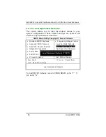
Page 59: ...5V 3 3V 5V 12V Move Enter Select PU PD Value F10 Save ESC Exit F1 General Help F5 Previous Values F6 Fail Safe Defaults F7 Optimized Defaults Current CPU Temp Show you the current CPU temperature Current System Temperature These read only fields reflect the functions of the hardware thermal sensor that monitors the chip blocks and system temperatures to ensure the system is stable Current CPUFAN1 ...

Page 60: ...ptimized Defaults Auto Detect DIMM PCI Clk This item automatically detects the clock speeds of the system memory installed as well as the PCI interface The options available are Enabled and Disabled The default setting is Enabled Speed Spectrum This item directly relates to the EMI performance of the whole system When enabled all system clocks run at slower speeds thereby decreasing the electromag...

Page 61: ...s CMOS Setup Utility Copyright Award Software Standard CMOS Features Frequency Voltage Control Advanced BIOS Features Load Fail Safe Defaults Advanced Chipset Features Load Optimized Defaults Integrated Peripherals Set Supervisor Password Power Ma PnP PCI C Load Fail Safe Defaults Y N N PC Health Status Exit Without Saving Esc Quit Select Item F10 Save Exit Setup Load Fail Safe Defaults To load BI...

Page 62: ...ility Copyright Award Software Standard CMOS Features Frequency Voltage Control Advanced BIOS Features Load Fail Safe Defaults Advanced Chipset Features Load Optimized Defaults Integrated Peripherals Set Supervisor Password Power Man PnP PCI Co Load Optimized Defaults Y N N PC Health Status Exit Without Saving Esc Quit Select Item F10 Save Exit Setup Load Optimized Defaults To load SETUP defaults ...

Page 63: ...g N brigs you back to Setup utility CMOS Setup Utility Copyright Award Software Standard CMOS Features Frequency Voltage Control Advanced BIOS Features Load Fail Safe Defaults Advanced Chipset Features Load Optimized Defaults Integrated Peripherals Set Supervisor Password Power Man PnP PCI Con SAVE to CMOS and EXIT Y N Y PC Health Status Exit Without Saving Esc Quit Select Item F10 Save Exit Setup...

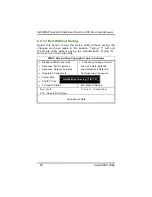
Page 64: ...fications Typing N will return you to Setup utility CMOS Setup Utility Copyright Award Software Standard CMOS Features Frequency Voltage Control Advanced BIOS Features Load Fail Safe Defaults Advanced Chipset Features Load Optimized Defaults Integrated Peripherals Set Supervisor Password Power Man PnP PCI Con Quit Without Saving Y N N PC Health Status Exit Without Saving Esc Quit Select Item F10 S...

Page 65: ...ing on the settings made on jumper JP3 of SBC82621 Follow the steps below to enable and program the watchdog function of SBC82621 Start Un Lock WDT OUT 120H 0AH enter WDT function OUT 120H 0BH enable WDT function Set multiple 1 4 OUT 120 0NH N 1 2 3 or 4 Set base timer 0 F OUT 121 0MH M 0 1 2 F WDT counting re set timer OUT 121 0MH M 0 1 2 F IF No re set timer WDT time out generate RESET or NMI IF...

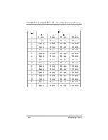
Page 66: ...50 secs 500 secs 5 3 secs 30 secs 300 secs 600 secs 6 3 5 secs 35 secs 350 secs 700 secs 7 4 secs 40 secs 400 secs 800 secs 8 4 5 secs 45 secs 450 secs 900 secs 9 5 secs 50 secs 500 secs 1000 secs A 5 5 secs 55 secs 550 secs 1100 secs B 6 secs 60 secs 600 secs 1200 secs C 6 5 secs 65 secs 650 secs 1300 secs D 7 secs 70 secs 700 secs 1400 secs E 7 5 secs 75 secs 750 secs 1500 secs F 8 secs 80 secs ...

Reviews: