background image

21

TB1 and J6 Power

The TB1 and J6 connectors provide power input to the board or if J6 is used for input, TB1
maybe used to source additional circuitry.  The J6 power jack accepts a standard 2.0 ~ 2.1mm
center barrel plug connector (positive voltage center) to provide the +VIN supply of +7 to +20
VDC @ 300ma minimum (+9VDC nominal).  TB1 provides access to the +VIN, GND (power
ground), and +5V power supplies.  The CMD912x power supply will provide 500ma of +5V for
user application.  +VIN input power should only be applied by J6 or TB1, not both or a supply
conflict may occur and the CMD912x board could be damaged.

BDM PORT

The BDM port on the PM12xxx module is a 6 pin header compatible with the Motorola
Background Debug Mode (BDM) Pod.  This allows the connection of a background debugger
for software development, programming and debugging in real-time without using HC12 I/O
resources.

BGND

1 2

GND

3 4

/RESET

5 6

+5V

See the HC12 Technical Reference Manual for complete
documentation of the BDM.

A Background Debug Module is available from the manufacturer.

Summary of Contents for MCU 68HC912

Page 1: ...ndustrial Ln Garland TX 75041 972 926 9303 FAX 972 926 6063 email Sales axman com web http www axman com xiom anufacturing CMD912x Development Board for Motorola 68HC912 MCU s 68HC912D60 DG128 DT128 and MC9S12DP256 ...

Page 2: ...10 PM12DG128 PM12DT128 Memory Map 11 PM12D60 Memory Map 12 OPTION SWITCHES 13 CONFIG SWITCH 13 COM SWITCH 13 MODE SWITCH 14 PORTS AND CONNECTORS 15 PRU PORT 15 PRU PORT CONNECTOR 16 MCU_PORT 1 16 MCU_PORT 2 17 BUS_PORT 17 ANALOG PORT 18 COM1 18 COM2 18 CAN1 4 PORTS 19 LCD_PORT 20 KEYPAD 20 TB1 and J6 Power 21 BDM PORT 21 TROUBLESHOOTING 22 TABLES 24 TABLE 1 LCD Command Codes 24 TABLE 2 LCD Charact...

Page 3: ...E requires you to specify your board You should select 912 xxx version of your development board Board Startup Follow these steps to connect and power on the board for the default Monitor operation This assumes you re using the provided AxIDE utility installed in the previous section or a similar communications terminal program on your PC If you re using a different terminal program than the one p...

Page 4: ...the disk are free assemblers the GNU C C compiler tools for HC12 example source code and other useful software The introductory tutorial in this manual uses the free AS12 assembler integrated into the AxIDE program This is a simple assembler with limited capability For a more powerful assembly tool install the Motorola MCUez program from the CD This will allow you to used PAGED memory in your appl...

Page 5: ... board s use of Memory and Addressing when writing source code so you can locate your code at valid addresses For example when in debug mode you should put your program CODE in External RAM In assembly language you locate the code with ORG statements in your source code Any lines following an ORG statement will begin at that ORG location which is the first number following the word ORG for example...

Page 6: ... with this board contains a simple interface to this assembler Use it by selecting Build from its menu This will prompt you for the file to be assembled NOTE You must select your board from the pull down menu first or it may not build correctly DO NOT use long path names 8 characters The free assembler is an old DOS tool that does not recognize them If there are no errors in your source code 2 out...

Page 7: ...xecute the program at address 4400 which is the start of our test program 5 If everything is working properly you should see the message Hello World echoed back to your terminal screen Press RESET to return to the monitor 6 If you do not get this message see the TROUBLESHOOTING section in this manual You can modify the hello program to display other strings or do anything you want The procedures f...

Page 8: ... to go to the beginning of the program the label START when powered on org fffe reset vector fdb START 5 Re Assemble HELLO ASM as described in the Assembling Source Code section 6 Select Program from the AxIDE menu and follow the message prompts When prompted for a file name enter the new HELLO S19 file 7 Press the RESET button on the board before clicking OK When prompted to Erase choose Yes 8 Wh...

Page 9: ...ation with the ECS enabled for Paging emulation 2 PM12xxx MODE SWITCH is usually set for positions 1 and 2 off to select Single Chip Mode This setting forces the BDM Monitor in the HC12 active immediately after Reset with the BDM connected which is desired for most BDM pods The BDM can then load a script to set the desired operating mode and configuration see next note The DP256 version should hav...

Page 10: ...Expanded Wide Mode Single Chip Mode C000 1 2 3 CONFIG ON ON OFF MODE ON ON ON External EPROM U5 6 Mon12 1 2 3 4 CONFIG OFF OFF OFF OFF MODE OFF OFF OFF On Chip Flash Memory Flash Page 8000 C000 BFFF 8000 4000 External RAM U3 4 1 2 3 CONFIG ON OFF MODE OFF OFF ON see BDM notes External RAM U3 4 3FFF 1000 On Chip RAM 3E00 3FFF used by Mon12 FFF 800 On Chip EEPROM 7FF 000 Internal Registers See your ...

Page 11: ... RAM U3 4 3FFF 2000 On Chip RAM 3E00 3FFF used by Mon12 1FFF 1000 Reserved FFF 800 On Chip EEPROM Peripheral Area 7FF 400 Unused 400 7BF LCD CS7 7F0 7FF CS6 7E0 7EF CS5 7D0 7DF CS4 7C0 7CF CS3 7B0 7BF CS2 7A0 7AF CS1 790 79F CS0 780 78F 3FF 000 Internal Registers See your MCU Technical Reference Manual 1 The Peripheral Area A00 BFF is set to Narrow 8 bit data width by the debug utilities If using ...

Page 12: ... B90 B9F CS0 B80 B8F 9FF 800 Internal Registers see note 1 below See 68HC912D60 Technical Reference Manual 7FF 000 Internal RAM On Chip 2 The Internal Register base address is relocated from 000 to 800 on startup by the debug utilities Mon12 and NoICE To preserve this memory map you must also do this in your software when booting from flash To do this load register 11 with 08 for example MOVB 08 1...

Page 13: ...TCH position 1 is also on When in off position memory space is SRAM for BDM use COM SWITCH The 6 position COM SWITCH on the CMD912x Board provides an easy method of connecting or isolating the HC12 SCI and CAN channel RXD pins from the provided on board transceivers The HC12 SCI channels are connected to RS232 transceivers and the first 4 CAN channels are connected to 1M baud CAN transceivers To a...

Page 14: ...Mode Single Chip Mode Expanded Wide Mode 3 Port H pull device Port H Pull Down Port H Pull Up 4 Port G pull device Port G Pull Down Port G Pull Up 5 Oscillator Select Ext 16Mhz Clock User applied crystal PM12DG128 PM12DT128 Default 1 and 2 ON 3 OFF MODE SWITCH SELECTION OPTION OFF POSITION ON POSITION 1 and 2 Operating Mode Single Chip Mode Expanded Wide Mode 3 Oscillator Select Ext 16Mhz Clock Us...

Page 15: ...ports The HC12 allows this to be optioned on input ports 3 The PRU will only drive outputs high to 4V The PRU port pull up resistors raise the output level to 5V with minimal drive 4 PRU port inputs will indicate logic high if not driven due to the pull up resistors The PRU will provide HC12 internal resource memory mapping support with constraints The user should be cautious to stay within the bo...

Page 16: ...7 18 PX7 PS6 19 20 PS7 PS4 21 22 PS5 PS2 23 24 PS3 PS0 25 26 PS1 PT0 27 28 PT1 PT2 29 30 PT3 PT4 31 32 PT5 PT6 33 34 PT7 PG PJ0 35 36 PG PJ1 PG PJ2 37 38 PG PJ3 PG PJ4 39 40 PG PJ5 PG PJ6 41 42 PG PJ7 PH6 43 44 PH7 PH4 45 46 PH5 PH2 47 48 PH3 PH0 49 50 PH1 The MCU_PORT1 provides access to the peripheral features and I O lines of the HC12 Note 1 Not all I O Ports are provided by all HC12 MCUs 2 The...

Page 17: ...4 A11 17 18 A5 A9 19 20 A6 A8 21 22 A7 A12 23 24 A13 WE 25 26 CS0 CS1 27 28 CS2 CS3 29 30 CS4 CS5 31 32 IRQ 5V 33 34 P SEL RW 35 36 CS6 E 37 38 CS7 GND 39 40 RESET The BUS_PORT supports off board memory devices D8 D15 High Byte Data Bus in Wide Expanded Mode and Peripheral 8 bit data bus Port A in Single Chip Mode A0 A13 Memory Addresses 0 to 13 OE Memory Output Enable signal Active Low Valid with...

Page 18: ... 3 4 RXD1 5 6 7 8 GND 9 10 The COM 2 has a Female DB9 connector that interfaces to the HC12 internal SCI1 serial port It uses a simple 2 wire asynchronous serial interface and is translated to RS232 signaling levels JP1 may be used to reverse RS232 RX and TX signals to the COM2 connector NOTE 1 COM1 and 2 connector Pins 1 4 and 6 are connected for default handshake standards 2 COM1 and 2 connector...

Page 19: ...e CMD912x board near the respective CAN port CAN Bus transceiver transmit enable control can be applied to each CAN 1 4 Port by the RS1 4 tie pads respectfully The user should select an available HC12 I O port to perform the transmit enable function and connect it from the MCU_PORTx pin to RSx pad as required The RC10 RC20 RC30 or RC40 resistors must be removed from the respective CAN port to appl...

Page 20: ...1 D12 D15 14 13 D14 Command Register LCD PORT Base 0 Data Register LCD PORT Base 1 LCD Vee is supplied by U16 and is adjusted by the CONTRAST Potentiometer adjustable resistor See the file KLCD12Dx ASM for an example program using this LCD connector J3 LCD3 2 1 LCD2 4 3 LCD4 Additional lines can be used as enables for larger character panels and are mapped as LCD2 Base 4 5 LCD4 Base C D LCD3 Base ...

Page 21: ... will provide 500ma of 5V for user application VIN input power should only be applied by J6 or TB1 not both or a supply conflict may occur and the CMD912x board could be damaged BDM PORT The BDM port on the PM12xxx module is a 6 pin header compatible with the Motorola Background Debug Mode BDM Pod This allows the connection of a background debugger for software development programming and debuggin...

Page 22: ...sure approximately 9 volts between the GND and VIN connections on the TB1 power connector with the standard power supply provided 4 If no voltage is found verify the wall plug connections to 115VAC outlet and the power connector 5 Verify the logic power source You should measure 5 volts between the GND and 5V connections on the TB1 power connector If the VIN supply is good and this supply is not 5...

Page 23: ... switch changes the memory map If debugging under Mon12 make sure you re not over writing RAM used by it If you re running in a multi tasking environment such as Windows close all programs in the background to be certain no serial conflict occurs Code Execution Make sure the CONFIG SWITCH is set for the proper mode CONFIG switch 3 must be ON to access the external bus LCD display etc even if execu...

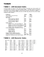
Page 24: ... 40us Display on Cursor and Cursor Blink off 0C 40us Display and Cursor on Cursor Blink off 0E 40us Display Cursor and Cursor Blink on 0F 40us Cursor Display Shift nondestructive move Cursor shift left 10 40us Cursor shift right 14 40us Display shift left 18 40us Display shift right 1C 40us Display Function default 2x40 size 3C 40us Character Generator Ram Address set 40 7F 40us Display Ram Addres...

Page 25: ...ation or Examine Modify same location or Examine Modify previous location Exit Modify Memory command MOVE StartAddress EndAddress DestAddress Move a block of memory RD Display all CPU registers RM Modify CPU Register Contents STOPAT Address Trace until address T count Trace count instructions 1 Mon12 uses internal RAM space from 600 7FF for the D60 and 3E00 3FFF for the DG128 and DP256 DO NOT use ...

Page 26: ...TRB PE3 LSTRB J1 P1 57 MCU PORT2 18 PE4 ECLK PE4 ECLK PE4 ECLK J1 P1 44 BUS PORT 37 PE5 MODA PE5 MODA PE5 MODA J1 P1 43 MCU PORT2 20 PE6 MODB PE6 MODB PE6 MODB J1 P1 42 MCU PORT2 17 PE7 DBE PE7 DBE PE7 J1 P1 41 MCU PORT2 22 PG0 PJ0 PJ0 J1 P1 26 MCU PORT1 35 PG1 PJ1 PJ1 J1 P1 25 MCU PORT1 36 PG2 PJ2 J1 P1 24 MCU PORT1 37 PG3 PJ3 J1 P1 23 MCU PORT1 38 PG4 PJ4 J1 P1 14 MCU PORT1 39 PG5 PJ5 J1 P1 13 M...

Page 27: ...CU PORT1 5 PP3 PWM3 PP3 PWM3 PP3 PWM3 J2 P2 3 MCU PORT1 6 PP4 PWM4 J2 P2 6 MCU PORT1 7 PP5 PWM5 J2 P2 5 MCU PORT1 8 PP6 PWM6 J2 P2 8 MCU PORT1 9 PP7 PWM7 J2 P2 7 MCU PORT1 10 BGND BGND BGND MODC J1 P1 27 BDM PORT RESET RESET RESET J1 P1 47 BUS PORT 40 BDM PORT PAD0 AN0 PAD0 AN0 PAD0 AN0 J2 P2 47 ANALOG PORT 1 PAD1 AN1 PAD1 AN1 PAD1 AN1 J2 P2 45 ANALOG PORT 3 PAD2 AN2 PAD2 AN2 PAD2 AN2 J2 P2 43 ANA...

Reviews: