3
Schematics
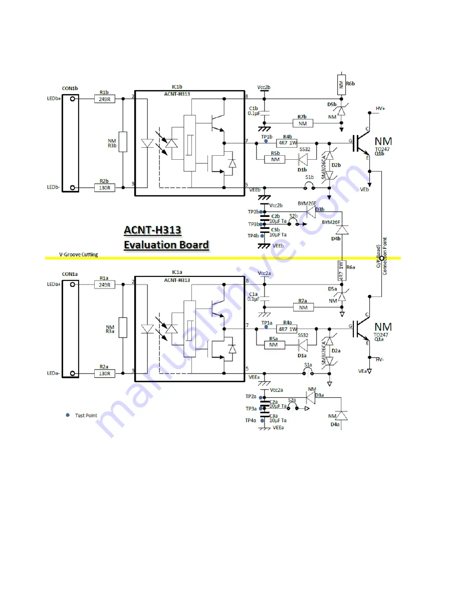
Figure 3 shows the schematics of the evaluation board:
Figure 3. Schematics of ACNT-H313 evaluation board
Page 1: ...eeded to generate the bias current across D5 3 The S1 jumper is shorted by default to connect VE to VEE assuming that a negative supply is not needed Note If a negative supply is needed then the S1 ju...
Page 2: ...crocontroller output to drive the lower arm of the half bridge inverter b Another 10 kHz 5 V DC pulse at 180 out of phase to 3a from the dual output signal generator across IN2 and IN2 pins of CON1b t...
Page 3: ...3 Schematics Figure 3 shows the schematics of the evaluation board Figure 3 Schematics of ACNT H313 evaluation board...
Page 4: ...pins IN2 and IN2 of CON1b of the top inverter arm isolated driver 4 Use a multi channel digital oscilloscope to capture the waveforms at the following points a LED signal at IN1 pin w r t IN1 for the...
Page 5: ...market Each of the ACNT H313 evaluation boards as shown in Figure 5 accommodates two units of ACNT H313 ICs Therefore each board is enough to drive the top and bottom arms of the half bridge inverter...
Page 6: ...signal input 1 If you require details of bootstrapping operation contact Avago Scheme 3 is similar to Scheme 1 it uses two external isolated supplies at VCC2a and VCC2b Scheme 3 however has the advan...
Page 7: ...ed but with Q1a and Q1b switchers mounted The switchers have a gate capacitance equivalent to 10 nF Figure 6 Input LED signals and switchers gate voltage waveforms Note Both IN1 and IN2 are set at 49...
Page 8: ...the turn off gate signal of Q1b Figure 8 Turn on and turn off gate waveforms of Q1a and Q1b Figure 7 and Figure 8 show that the turn off speed of the switchers is about 200 ns due largely to the capac...