background image

Confidentiality Status

This document is Non-Confidential. The right to use, copy and disclose this document may be subject to license restrictions in
accordance with the terms of the agreement entered into by Arm and the party that Arm delivered this document to.

Unrestricted Access is an Arm internal classification.

Product Status

The information in this document is Final, that is for a developed product.

Web Address

www.arm.com

Conformance Notices

This section contains conformance notices.

Federal Communications Commission Notice

This device is test equipment and consequently is exempt from part 15 of the FCC Rules under section 15.103 (c).

Class A

Important: This is a Class A device. In residential areas, this device may cause radio interference. The user should take the
necessary precautions, if appropriate.

CE Conformity


The 

Waste Electrical and Electronic Equipment

 (WEEE) marking, that is, the crossed out wheelie-bin figure, indicates that this

product must not be disposed of with general waste within the European Union. To prevent possible harm to the environment from
uncontrolled waste disposal, the user is required to recycle the product responsibly to promote reuse of material resources. To
comply with EU law, you must dispose of the product in one of the following ways:

Return it to the distributer where it was purchased. The distributer is required to arrange free collection when requested.

Recycle it using local WEEE recycling facilities. These facilities are now very common and might provide free collection.

If purchased directly from Arm, Arm provides free collection. Please e-mail 

[email protected]

 for instructions.

The CE Declaration of Conformity for this product is available on request.

The system should be powered down when not in use.

It is recommended that ESD precautions be taken when handling this product.

The product generates, uses, and can radiate radio frequency energy and may cause harmful interference to radio communications.
There is no guarantee that interference will not occur in a particular installation. If this equipment causes harmful interference to
radio or television reception, which can be determined by turning the equipment off or on, you are encouraged to try to correct the
interference by one or more of the following measures:

Ensure attached cables do not lie across any sensitive equipment.

Reorient the receiving antenna.

Increase the distance between the equipment and the receiver.

Connect the equipment into an outlet on a circuit different from that to which the receiver is connected.

Consult the dealer or an experienced radio/TV technician for help.


Note


It is recommended that wherever possible shielded interface cables be used.

 Arm

®

 DSTREAM-PT


101714_0100_02_en

Copyright © 2019 Arm Limited or its affiliates. All rights reserved.

3

Non-Confidential

Summary of Contents for DSTREAM-PT

Page 1: ...Arm DSTREAM PT Version 1 0 System and Interface Design Reference Guide Copyright 2019 Arm Limited or its affiliates All rights reserved 101714_0100_02_en ...

Page 2: ...BLE FOR ANY DAMAGES INCLUDING WITHOUT LIMITATION ANY DIRECT INDIRECT SPECIAL INCIDENTAL PUNITIVE OR CONSEQUENTIAL DAMAGES HOWEVER CAUSED AND REGARDLESS OF THE THEORY OF LIABILITY ARISING OUT OF ANY USE OF THIS DOCUMENT EVEN IF ARM HAS BEEN ADVISED OF THE POSSIBILITY OF SUCH DAMAGES This document consists solely of commercial items You shall be responsible for ensuring that any use duplication or d...

Page 3: ...distributer where it was purchased The distributer is required to arrange free collection when requested Recycle it using local WEEE recycling facilities These facilities are now very common and might provide free collection If purchased directly from Arm Arm provides free collection Please e mail weee arm com for instructions The CE Declaration of Conformity for this product is available on reque...

Page 4: ...s 1 24 1 7 Target Voltage Reference VTREF signals 1 26 1 8 I O diagrams for DSTREAM PT signals 1 28 1 9 Typical SWD circuit 1 30 1 10 Typical JTAG circuit 1 31 Chapter 2 Target interface connectors 2 1 Target connector selection guide 2 34 2 2 Arm JTAG 20 connector 2 35 2 3 CoreSight 10 connector 2 36 2 4 CoreSight 20 connector 2 37 2 5 TI JTAG 14 connector 2 39 2 6 Mictor 38 connector 2 40 101714...

Page 5: ...2 11 User I O connector 2 50 Chapter 3 Target board design 3 1 Overview of high speed design 3 52 3 2 JTAG port buffering 3 55 3 3 Series termination 3 58 3 4 Parallel trace modeling 3 59 3 5 Target design checklist 3 60 101714_0100_02_en Copyright 2019 Arm Limited or its affiliates All rights reserved 5 Non Confidential ...

Page 6: ...mple reset circuit 1 20 Figure 1 9 SWD timing diagrams 1 22 Figure 1 10 TRACECLK timing diagram 1 25 Figure 1 11 Target interface logic levels 1 27 Figure 1 12 Input Output signals 1 28 Figure 1 13 TCK signal 1 28 Figure 1 14 Reset signals 1 28 Figure 1 15 Trace signals 1 29 Figure 1 16 VTREF signals 1 29 Figure 1 17 Typical SWD circuit 1 30 Figure 1 18 Typical JTAG circuit 1 31 Figure 2 1 Arm JTA...

Page 7: ...th 3 52 Figure 3 3 Long stub causing false edges 3 53 Figure 3 4 Improved route with shorter stub 3 53 Figure 3 5 JTAG connection without buffers 3 55 Figure 3 6 JTAG connection with TDO buffer 3 55 Figure 3 7 Daisy chained JTAG connection without buffers 3 55 Figure 3 8 Daisy chained JTAG connection with TCK buffers 3 56 Figure 3 9 Fully buffered JTAG connection 3 56 101714_0100_02_en Copyright 2...

Page 8: ...rm CoreSight 20 pinout table DSTREAMCS20 0 2 37 Table 2 5 Arm CoreSight 20 pinout table DSTREAMCS20 1 2 38 Table 2 6 TI JTAG 14 pinout table 2 39 Table 2 7 Mictor 38 pinout table 2 40 Table 2 8 Mictor B pinout table 2 44 Table 2 9 MIPI 34 pinout table 2 45 Table 2 10 MIPI 60 pinout table 2 47 Table 2 11 User I O pinout table 2 50 Table 3 1 Typical series terminating resistor values 3 58 Table 3 2 ...

Page 9: ...roduces the Arm DSTREAM PT System and Interface Design Reference Guide It contains the following About this book on page 10 101714_0100_02_en Copyright 2019 Arm Limited or its affiliates All rights reserved 9 Non Confidential ...

Page 10: ...ssary is a list of terms used in Arm documentation together with definitions for those terms The Arm Glossary does not contain terms that are industry standard unless the Arm meaning differs from the generally accepted meaning See the Arm Glossary for more information Typographic conventions italic Introduces special terminology denotes cross references and citations bold Highlights interface elem...

Page 11: ...ts on content then send an e mail to errata arm com Give The title Arm DSTREAM PT System and Interface Design Reference Guide The number 101714_0100_02_en If applicable the page number s to which your comments refer A concise explanation of your comments Arm also welcomes general suggestions for additions and improvements Note Arm tests the PDF only in Adobe Acrobat and Acrobat Reader and cannot g...

Page 12: ... 10K is recommended Unless otherwise specified any signals beginning with a lowercase n are by default active LOW It contains the following sections 1 1 JTAG signals on page 1 13 1 2 Return Clock RTCK signal on page 1 18 1 3 Reset signals on page 1 19 1 4 Run Control signals on page 1 21 1 5 Serial Wire Debug SWD signals on page 1 22 1 6 Trace signals on page 1 24 1 7 Target Voltage Reference VTRE...

Page 13: ...ynchronizes its JTAG state machine On each rising edge of the TCK signal the target samples the TDI and TMS signals Consider TCK as a strobe signal rather than a clock signal because it is typically non continuous and only becomes active during debug communications TCK can be pulled HIGH on the target however to maintain full compatibility with other JTAG equipment Arm recommends you pull TCK LOW ...

Page 14: ...received by the devices For more information see JTAG port buffering on page 3 55 JTAG timing characteristics The JTAG timing characteristics of DSTREAM PT systems conform to the requirements of the IEEE 1149 1 JTAG specification TDI and TMS are set up by the DSTREAM PT system on the falling edge of TCK These signals are then sampled by the target device on the rising edge of TCK The target device...

Page 15: ...re no separate timing requirements for the adaptive clocking mode In adaptive clocking mode the debug unit samples TDO on the rising edge of RTCK instead of TCK so TDO timing is relative to RTCK Table 1 1 JTAG timing Characteristics Parameter Min Max Description F clk 10Hz 180MHz TCK frequency T clk 5 556ns 100ms TCK period T ds 49 51 TCK Duty Cycle For further details on the JTAG interface a full...

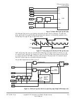
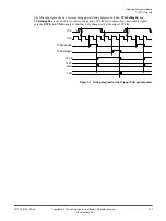
Page 16: ...e clocked by one edge of a single clock To interface the clocking restriction to a JTAG port that is asynchronous to the system you must convert the JTAG TCK events into clock enables for this single clock You must also ensure that the JTAG port cannot overrun this synchronization delay One possible implementation of this circuit is CKEN IN nRESET TMS CKEN TAP Ctrl State Machine OUT Scan Chain CKE...

Page 17: ...ow these enable signals gate the RTCK and TDO signals so that they only change state at the edges of TCK CLK TCKRisingEn TCK TCKFallingEn RTCK TAPC State TDO Figure 1 7 Timing diagram for the D type JTAG synchronizer 1 Debug and trace interface 1 1 JTAG signals 101714_0100_02_en Copyright 2019 Arm Limited or its affiliates All rights reserved 1 17 Non Confidential ...

Page 18: ...e flow of the JTAG interface as required Note If you use the adaptive clocking feature then the transmission delays gate delays and synchronization requirements might result in a lower clock frequency compared to using fixed clocking Adaptive clocking mode is not recommended unless the target design requires it Adaptive clocking can be enabled using the configuration settings in Arm Development St...

Page 19: ...RST signal HIGH The polarity of the nTRST signal is configurable in Arm Development Studio Note Arm strongly recommends that the nSRST and nTRST signals are separately available on the JTAG connector If the nSRST and nTRST signals are linked together resetting the system also resets the TAP controller which means Depending on your target it might not be possible to debug a system from reset becaus...

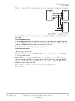
Page 20: ...ed on development boards The reset device that is shown here would keep the target device and any other system devices in their reset state until the power rail has reached a minimum valid voltage If the target device has a separate Power On Reset POR input any voltage monitoring devices would typically connect to that instead If the target device is equipped with internal voltage monitoring circu...

Page 21: ... on the target board Warning If the signal is used it must be pulled LOW on the target Debug Acknowledge DBGACK The Debug Acknowledge DBGACK pin notifies the debug unit that a debug request has been received and that the target processor is now in its debug state Arm recommends that this signal is no longer used It can be left open on the target board Warning If the signal is used it must be pulle...

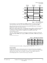
Page 22: ... Serial Wire Output SWO The Serial Wire Output SWO signal is an output from the target which is often used alongside the SWD signals to provide low bandwidth trace The SWO signal must be pulled HIGH on the target to keep the signal inactive when no debug unit is connected SWD timing requirements The diagrams that are shown in the following figure separate the SWDIO line to show when it is driven b...

Page 23: ...igh 4ns 50ms SWCLKHIGH period T low 4ns 50ms SWCLKLOW period T os 1ns 1ns SWDIO output skew to falling edge SWCLK T is 4ns Input setup time that is required between SWDIO and rising edge SWCLK T ih 1ns Input hold time that is required between SWDIO and rising edge SWCLK 1 Debug and trace interface 1 5 Serial Wire Debug SWD signals 101714_0100_02_en Copyright 2019 Arm Limited or its affiliates All ...

Page 24: ...pture of up to 4 bit wide continuous mode Trace Port Interface Unit TPIU formatted trace at up to 600Mbps per trace signal The Parallel Trace probe in the DSTREAM PT system extends this functionality by supporting up to 32 bit wide TPIU trace The trace signals supported by DSTREAM PT are TRACEDATA 0 31 The Trace Data signals are outputs from the target and can be used to collect 1 bit to 32 bit tr...

Page 25: ...A and TRACECLK outputs close to the target device The value of these resistors added to the impedance of the driver must be approximately equal to 50Ω To achieve the maximum data rate Arm recommends using the short 20 way 0 05 pitch ribbon cable The following figure and table describe the timing for TRACECLK Tperiod Twh Twl Figure 1 10 TRACECLK timing diagram Table 1 3 TRACECLK characteristics Par...

Page 26: ...bug and trace signals Arm recommends connecting VTREF signals directly to one or more appropriate power rails on the target board If a series resistor is used for short circuit protection the value used must be less than 100Ω VTREF signals that are received by the DSTREAM PT system are loaded with a resistance of approximately 10K to ground The signals are filtered limited and buffered to provide ...

Page 27: ...nput and output characteristics of the DSTREAM PT system are compatible with logic levels from TTL compatible or CMOS logic in target systems 1 Debug and trace interface 1 7 Target Voltage Reference VTREF signals 101714_0100_02_en Copyright 2019 Arm Limited or its affiliates All rights reserved 1 27 Non Confidential ...

Page 28: ...signals TCK signal The TCK output signal is similar to a standard output signal but also has a switchable capacitor forming a T filter which can reduce the TCK slew rate Enabling this filter is not currently supported in Arm Development Studio 16 5R 220pF 16 5R Figure 1 13 TCK signal Reset signals The reset signals nSRST and nTRST are similar to the standard input output signals However they have ...

Page 29: ...R 50R VTREF 2 VTREF 2 Figure 1 15 Trace signals VTREF signals The VTREF signals VTREF DEBUG_VTREF and TRACE_VTREF are buffered to provide A VDD rail for the LVCMOS output buffers The VTREF 2 reference termination rail For the debug unit to detect that a target is present the VTREF signal must be higher than 800mV 33R 10K 5K 5K Target Detect Buffered VTREF VTREF 2 800mV Figure 1 16 VTREF signals 1 ...

Page 30: ...e To improve signal integrity it is good practice to provide an impedance matching resistor on the SWDIO and SWO outputs of the processor The value of these resistors added to the impedance of the driver must be approximately equal to 50Ω 1 Debug and trace interface 1 9 Typical SWD circuit 101714_0100_02_en Copyright 2019 Arm Limited or its affiliates All rights reserved 1 30 Non Confidential ...

Page 31: ...al JTAG circuit Note To improve signal integrity it is good practice to provide an impedance matching resistor on the TDO and RTCK outputs of the processor The value of these resistors added to the impedance of the driver must be approximately equal to 50Ω 1 Debug and trace interface 1 10 Typical JTAG circuit 101714_0100_02_en Copyright 2019 Arm Limited or its affiliates All rights reserved 1 31 N...

Page 32: ...g a volume order of Arm debug units contact Arm support with your requirements Arm might be able to supply a compatible adapter on a fast turn prototype basis Note All connector pinouts in this chapter are shown as they would appear on the target board It contains the following sections 2 1 Target connector selection guide on page 2 34 2 2 Arm JTAG 20 connector on page 2 35 2 3 CoreSight 10 connec...

Page 33: ... 2 11 User I O connector on page 2 50 2 Target interface connectors 101714_0100_02_en Copyright 2019 Arm Limited or its affiliates All rights reserved 2 33 Non Confidential ...

Page 34: ...Low High Low Medium Connector durability 2 High Low Low High Medium Low Medium Approximate footprint area mm 3 297 65 95 250 221 140 170 Through hole SMD Either Either Either Either SMD 4 Either SMD Ease of assembly placement soldering High High High High Low High Medium Note 1 The trace width supported by the connector DSTREAM ST supports up to 4 bit wide parallel trace DSTREAM PT supports up to ...

Page 35: ... JTAG 20 pinout table Pin Signal name Pin Signal name 1 VTREF 2 NC 3 nTRST 4 GND 5 TDI 6 GND 7 TMS SWDIO 8 GND 9 TCK SWCLK 10 GND 11 RTCK 12 GND 13 TDO SWO 14 GND 15 nSRST 16 GND 17 DBGRQ 18 GND 19 DBGACK 20 GND Warning Using a non shrouded header on the target board can lead to short circuits or signal contention To ensure the correct polarity and position Arm recommends that you use a fully shro...

Page 36: ... table Pin Signal name Pin Signal name 1 VTREF 2 TMS SWDIO 3 GND 4 TCK SWCLK 5 GND 6 TDO SWO 7 Key NC 8 TDI 9 GND 10 nSRST Note Pin 7 must be removed for compatibility with DSTREAM ST and MIPI specifications Warning Using a non shrouded header on the target board can lead to short circuits or signal contention To ensure the correct polarity and position Arm recommends that you use a fully shrouded...

Page 37: ...system is connected To configure the pinout mode use the Platform Configuration Editor PCE in Arm Development Studio In the PCE select Debug Adapter then select the Probe Configuration tab In the configuration items table set the DSTREAMCS20 configuration item to either 0 to use the connector in JTAG debug and trace mode 1 to use the connector in JTAG debug only mode For more information see Confi...

Page 38: ... pins are typically grounded on the target board the MIPI specification also allows them to carry power If they are connected to a power rail or rails on the target board these pins must also be AC coupled to GND To couple the pins to GND use 100nF capacitors that are close to the connector Note Pin 7 must be removed for compatibility with DSTREAM ST and MIPI specifications Warning Using a non shr...

Page 39: ...6 NC 7 TDO SWO 8 GND 9 RTCK 10 GND 11 TCK SWCLK 12 GND 13 DBGRQ 14 DBGACK Warning Using a non shrouded header on the target board can lead to short circuits or signal contention To ensure the correct polarity and position Arm recommends that you use a fully shrouded box header For the pin out of the TI JTAG 14 connector do not use 14 way IDC cables to connect the target board and debug unit To avo...

Page 40: ...plied 4 bit Mictor adapter must be used in conjunction with both the Arm JTAG 20 debug cable and the CoreSight 20 debug cable To use this connector with DSTREAM PT the supplied 16 bit Mictor adapter must be used in conjunction with the MIPI 60 cable 1 2 3 4 5 6 7 8 9 10 11 12 13 14 15 16 17 18 19 20 21 22 23 24 25 26 27 28 29 30 31 32 33 34 35 36 37 38 Figure 2 5 Mictor 38 connector pinout Mictor ...

Page 41: ...ment Studio 2 Although the Arm CoreSight specification only supports a single VTREF on pin 12 DSTREAM ST can support separate debug and trace VTREFs If only TRACE_VTREF is powered the DSTREAM ST assumes that both debug and trace are to operate at that voltage 3 These signals are not used by DSTREAM ST To maintain compatibility with other debug units connect the signals to the appropriate power rai...

Page 42: ...nnector If you do not solder paste on the same side of the PCB as the connector it might cause mechanical or signal integrity issues Typically the sockets used are a 2 767004 2 from TE Connectivity To use these connectors with DSTREAM PT the supplied 32 bit Mictor adapter must be used in conjunction with the MIPI 60 cable 2 Target interface connectors 2 7 Dual Mictor connectors 101714_0100_02_en C...

Page 43: ... 9 10 11 12 13 14 15 16 17 18 19 20 21 22 23 24 25 26 27 28 29 30 31 32 33 34 35 36 37 38 MICTOR A MICTOR B 1 35 34 29mm Figure 2 6 Dual Mictor connector pinout 2 Target interface connectors 2 7 Dual Mictor connectors 101714_0100_02_en Copyright 2019 Arm Limited or its affiliates All rights reserved 2 43 Non Confidential ...

Page 44: ...RACEDATA 22 19 NC 20 TRACEDATA 21 21 NC 22 TRACEDATA 20 23 TRACEDATA 31 24 TRACEDATA 19 25 TRACEDATA 30 26 TRACEDATA 18 27 TRACEDATA 29 28 TRACEDATA 17 29 TRACEDATA 28 30 Logic 0 1 31 TRACEDATA 27 32 Logic 0 1 33 TRACEDATA 26 34 Logic 1 1 35 TRACEDATA 25 36 Logic 0 1 37 TRACEDATA 24 38 TRACEDATA 16 Note 1 These signals are not used by Arm debug units To maintain compatibility with other debug unit...

Page 45: ...rds The MIPI 34 adapter and debug cable is not supplied with the DSTREAM ST unit but are available on request 1 2 3 4 5 6 8 9 10 7 11 12 13 14 15 16 17 18 19 20 21 22 23 24 25 26 27 28 29 30 31 32 33 34 Figure 2 7 MIPI 34 connector pinout MIPI 34 pinout table Table 2 9 MIPI 34 pinout table Pin Signal name Pin Signal name 1 DEBUG_VTREF 2 TMS SWDIO 3 GND 4 TCK SWCLK 5 GND 6 TDO SWO 7 Key NC 8 TDI 9 ...

Page 46: ... using 100nF capacitors that are close to the connector 2 The TRST_PD signal allows the target board to have a second TAP reset signal which is normally pulled down For more information see the MIPI debug connector specification 3 The TRACEEXT signal is not supported by DSTREAM ST Note Pin 7 must be removed for compatibility with DSTREAM ST and MIPI specifications Warning Using a non shrouded head...

Page 47: ...bug and trace signals It is necessary to supply the appropriate voltages to both of the VTREF pins 1 2 59 60 Figure 2 8 MIPI 60 connector pinout MIPI 60 pinout table Table 2 10 MIPI 60 pinout table Pin Signal name Pin Signal name 1 DEBUG_VTREF 2 TMS SWDIO 3 TCK 4 TDO 5 TDI 6 nSRST 7 RTCK 8 TRST_PD 1 9 nTRST 10 DBGRQ 11 DBGACK 12 TRACE_VTREF 13 TRACECLK 0 14 RESERVED 15 GND 16 GND 17 TRACECTL 18 TR...

Page 48: ... 47 TRACEDATA 14 48 RESERVED 49 TRACEDATA 15 50 RESERVED 51 TRACEDATA 16 52 RESERVED 53 TRACEDATA 17 54 RESERVED 55 TRACEDATA 18 56 RESERVED 57 GND 58 GND 59 RESERVED 60 RESERVED Note 1 The TRST_PD signal allows the target board to have a second TAP reset signal which is normally pulled down For more information see the MIPI debug connector specification Note DSTREAM ST only supports one channel o...

Page 49: ... or PCIe Warning This connector is not intended for user I O Do not attempt to connect anything other than Arm DSTREAM ST compatible probes This connector is not compatible with older RealView Trace RVT probes 2 Target interface connectors 2 10 Auxiliary AUX connector 101714_0100_02_en Copyright 2019 Arm Limited or its affiliates All rights reserved 2 49 Non Confidential ...

Page 50: ...Output 3 4 Output 4 5 Output 5 6 Input 1 7 Output 6 8 Input 2 9 3 3V output 10 GND Note User outputs use the 3 3V LVCMOS standard and have a 100R series resistor for short circuit protection User inputs use the 3 3V LVCMOS standard and have a 10K series resistor and 100K pull up resistor The inputs can be safely driven up to a maximum of 5V The 3 3V power output can be used to supply external circ...

Page 51: ...s chapter It contains the following sections 3 1 Overview of high speed design on page 3 52 3 2 JTAG port buffering on page 3 55 3 3 Series termination on page 3 58 3 4 Parallel trace modeling on page 3 59 3 5 Target design checklist on page 3 60 101714_0100_02_en Copyright 2019 Arm Limited or its affiliates All rights reserved 3 51 Non Confidential ...

Page 52: ... signals TCK RTCK and TRACECLK Avoid stubs Where possible debug and trace signals should be point to point between the driver and receiver of the signal with no T junctions or branches leading to other circuitry on the target board Target Device Debug Connector Figure 3 1 Point to point signal For debug signals pull up or pull down resistors are often required Pull up or pull down resistors might ...

Page 53: ...for example JTAG and general I O To deflect a larger portion of the signal away from the stub use a resistor at the junction of the stub This method is used when the stub leads to lower bandwidth circuitry Ensure the continuity of return signals As a digital signal propagates along its route an inverse signal travels through the adjacent plane because of the electric field coupling between the sig...

Page 54: ...urther apart than they are from the nearest plane the 3W rule Bring the plane closer to the signals To reduce the 3W distance that is needed between adjacent signals use thinner laminates between the signal and plane layers Keep the signal tracks as short as possible To cut down on routing while also reducing crosstalk place a debug or trace connector closer to the target device Use impedance matc...

Page 55: ...t option and achieves good signal integrity because each signal is point to point However if the TDO output of the target device has a weak drive strength 4mA the TDO output could significantly limit the maximum frequency of the JTAG interface To resolve this place a buffer close to the TDO pin of the target device with the appropriate series termination resistor Target Device Debug Connector TDI ...

Page 56: ... TDI TMS TCK TDO Target Device TDI TMS TCK TDO Target Device TDI TMS TCK TDO Figure 3 8 Daisy chained JTAG connection with TCK buffers The solution in the above figure prevents the two TCK branches from interacting and ensures good signal integrity with minimal overshoot You must place buffers and series termination resistors as close as possible to the T junction of the TCK signal This causes som...

Page 57: ...uffers can be used instead of standard buffers Arm recommends you use buffers with a drive strength of 24mA or above For any buffered signal place the signal pull up or pull down resistor at the input side of the buffer For guidance on selecting series termination resistors see Series termination on page 3 58 3 Target board design 3 2 JTAG port buffering 101714_0100_02_en Copyright 2019 Arm Limite...

Page 58: ...ions and target power usage The target signal impedance for DSTREAM ST is 50Ω When the outputs cannot be simulated typical series terminating resistor values are Table 3 1 Typical series terminating resistor values Driver strength Typical series terminator Notes 32mA 39Ω Best signal integrity highest speed 24mA 33Ω 16mA 27Ω 12mA 22Ω 8mA 15Ω 6mA 10Ω Worst signal integrity lowest speed Some types of...

Page 59: ...ch micro coaxial ribbon and can be modeled as a 50Ω transmission line with a 1 5ns propagation delay and 0 1Ω DC resistance The connectors at either end can be modeled as a 0 25pF capacitance to ground The circuit at the DSTREAM ST end of the transmission line can be modeled using the following primitives All resistors can be modeled as their ideal resistance values with minimum or zero parasitics...

Page 60: ...in 50Ω output impedance have you routed any outputs from the target device through series termination resistors Have the appropriate VTREF signal or signals been connected to the debug or trace connector or connectors Either directly or through a resistor of 100Ω or less are VTREF pins connected to the debug trace logic rail or rails Are the debug trace logic rails in the range of 1 2V to 3 3V Are...

Reviews: