Programmers Model
ARM DDI 0397G
Copyright © 2006-2010 ARM. All rights reserved.
3-5
ID031010
Non-Confidential
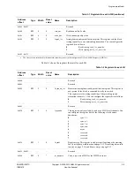
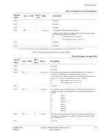
Table 3-2 shows the registers that exist for each IB.
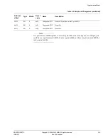
0x044
-
0x0FC
-
-
-
-
Reserved.
0x100
RW
4
0
read_qos
Read channel QoS value.
0x104
RW
4
0
write_qos
Write channel quality value.
0x108
RW
2
0
fn_mod_iss
Issuing functionality modification register. This register sets the block
issuing capability to one outstanding transaction. You can configure the
register bits as follows:
0
Read issuing,
read_iss_override
.
1
Write issuing,
write_iss_override
.
0x10C
-
0xFFC
-
-
-
-
Reserved.
a. The reset value is initialized to the tidemark value that you set in the configuration GUI in AMBA Designer (ADR-301).
Table 3-1 Registers for each ASIB (continued)
Address
offset
Type
Width
Reset
value
Name
Description
Table 3-2 Registers for each IB
Address
offset
Type
Width
Reset
value
Name
Description
0x000
-
-
-
-
Reserved.
0x004
-
-
-
-
Reserved.
0x008
RW
2
0
fn_mod_bm_iss
Bus matrix issuing functionality modification register. This register is
only present if the block is connected directly to a switch.
This register sets the issuing capability of the preceding switch
arbitration scheme to 1. You can configure the register bits as follows:
0
Read issuing,
read_iss_override
.
1
Write issuing,
write_iss_override
.
0x00C
-
-
-
-
Reserved.
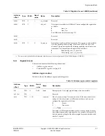
0x020
RW
3
4
Sync_mode
This register is only available if you have a FIFO for all channels. You
can configure the register bits for the following clock domain
boundaries:
0
sync 1:1.
1
sync n:1.
2
sync 1:n.
3
sync m:n.
4
async.
5
reserved.
6
reserved.
7
reserved.
0x024
RW
1
0
fn_mod2
Bypass merge. This register is only present if upsizing or downsizing.
See
Upsizing data width function
on page 2-12,
Downsizing data width
function
on page 2-14, and
Bypass merge
on page 2-13.
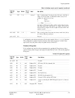
0x028
-
0x03C
-
-
-
-
Reserved.
0x040
RW
4
a
wr_tidemark
Value, only with a FIFO for the WFIFO channel.

