background image

writing to the data register at BASE+2 (Low nibble bits 0-3) and BASE + 3 (High byte bits 4-11). Prior

to this the DAC channel must be selected by writing a value of 02H to the Index register for DAC A

and 03H for DAC B.

Digital I/O

The APCI-ADADIO provides 16 digital I/O lines, these are grouped into four nibbles. Each nibble has

a power-up/reset state link and can be programmed as either input or output via the Digital I/O

configuration register. 
Access to the individual I/O lines is via Index registers 0AH and 0BH. Reading these registers will

provide the status of all I/O lines regardless of whether they are configured as input or output. It is

possible to use these lines as bi-directional with some careful programming ensuring that a conflict

does not exist on any of these lines.

Note:

- If a nibble is to be used as an input the reset state link must be set to the high position,

otherwise the lines will be driven low as outputs which may cause damage.

Counter/Timer

The APCI-ADADIO contains an 8254 compatible counter/timer, which provides three 16-bit

counter/timers. Channel 0 can be used to trigger an A/D conversion and channel 1 can cause an

interrupt request sequence to be initiated.
A external connector (PL3) has been provided to allow internal or external signals to be used as clock

sources. The connector has been arranged to allow the on-board 1Mhz clock to be connected to the

clock input on channel 1 and 2 via links. The outputs of these timers can also be cascaded to provide

longer timing sequences.
Counter 0 should always be programmed in mode 2 which ensures that  the output signal is only

active for a single clock cycle (i.e. 1uS when connected to the 1MHz clock). When the output from

counter 2 is used as the clock source the time between rising edges must not exceed 6 uS or be less

than 250nS.

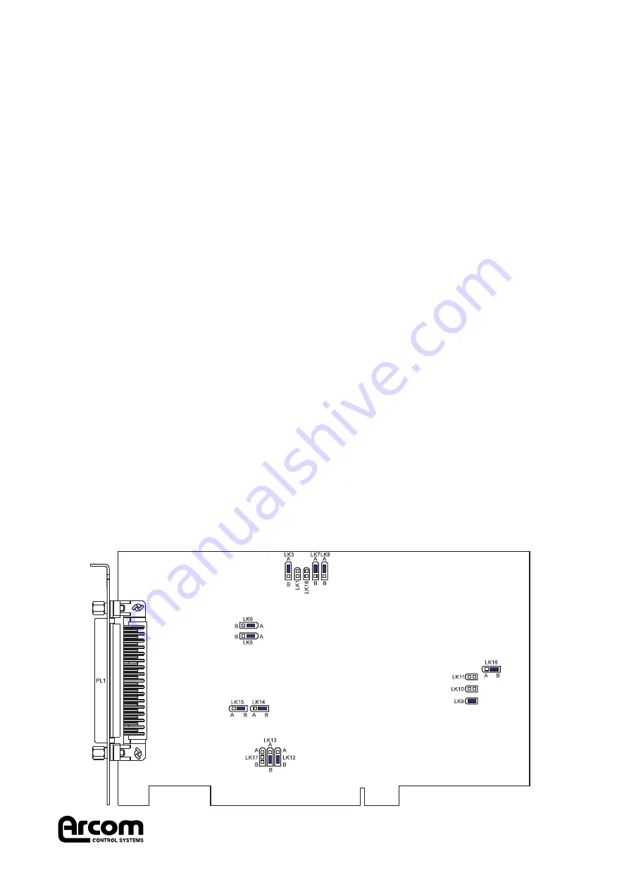
Links

Throughout this section a ‘+’ indicates the default link position.

Default Link Position Diagram

Page 5

2192-09125-000-000

J605 APCI-ADADIO

Summary of Contents for APCI-ADADIO

Page 1: ...ompatible 3 channel Counter timer 1 ADC Timer 1 Interrupt timer 1 general purpose timer 1MHz master operating frequency I O connector conforms to Arcoms signal conditioning system SCS Board Access LED RED User LED GREEN 32 bit PCI 2 1 Compatible Bus Interface Plug and Play Software compatible CE compliant design Operating Temperature range 0 C to 70 C Power consumption 180mA 5V 280mA 12V MTBF 220 ...

Page 2: ...PCI BIOS function calls I O Map The APCI ADADIO uses an indexed addressing scheme to access the on board devices and special function registers Two consecutive I O locations are required to implement this scheme the BASE address is used to set the index value and the BASE 1 address is used to access the device ADC and DAC data is accessed via a dedicated pair of registers which are not part of the...

Page 3: ... 3 Write Base 2 Write Base 3 Read Write Base 1 Read Write Base 1 Read Write Base 1 Write Base 1 Write Base 1 Write Base 1 Read Write Base 1 Read Write Base 1 N A Read Write Write Base 1 Read Base 1 Bit Function Bit 0 ADC Ready 0 Conversion completed since last read of ADC Data High byte Bit 1 Counter Timer Ready 0 OUT1 has transitioned low high since Clear CTC Ready was last accessed Bit 0 7 Any d...

Page 4: ...ulse 3 Periodic timer programmed from the on board counter timer channel 0 The following sequence can be used to perform an A D conversion when using the software trigger mode 1 Write 01H to the BASE address 2 Write to BASE 1 with the Multiplexer value for the appropriate channel 3 Wait for approximately 50uSec for the input to settle 4 Write 00H to the BASE address 5 Write to BASE 1 any value to ...

Page 5: ...ition otherwise the lines will be driven low as outputs which may cause damage Counter Timer The APCI ADADIO contains an 8254 compatible counter timer which provides three 16 bit counter timers Channel 0 can be used to trigger an A D conversion and channel 1 can cause an interrupt request sequence to be initiated A external connector PL3 has been provided to allow internal or external signals to b...

Page 6: ...t reset in nibble 4 bit groups The link associated with each nibble is shown below LK15 Digital I O lines 0 3 LK14 Digital I O lines 4 7 LK13 Digital I O lines 8 11 LK12 Digital I O lines 12 15 Note If a nibble is to be used as an Input the corresponding link should be placed in position B to ensure damage is not caused to the card or external circuitry LK16 Counter Timer Channel 0 clock source Th...

Page 7: ... the correct states and should be left in position A User Configuration Record Diagram Pseduo Differential Ground Differential Single Ended Input DAC Output range ADC Input Ranges ADC Trigger Sources Digital I O Reset State Counter Timer Channel 0 Clock Source Digital I O Reset Test Link LK1 LK3 LK5 LK6 LK7 LK8 LK18 LK9 LK10 LK11 LK12 LK13 LK14 LK15 LK16 LK17 ...

Page 8: ...igital voltmeter DVM with at least 5 digit resolution and a high stability low noise DC signal source During calibration it is necessary to continually read and display the ADC data A program ADADIO EXE has been provided on the utility disk to enable this Two trim adjusters VR7 and VR1 are provided for trimming the zero offset and gain respectively These trims are for fine adjusting the standard r...

Page 9: ... output to 000 hex 2 Measure the voltage between DAC A output and analogue ground and adjust VR5 to give 0 000V Full Scale Gain Adjust 1 Set DAC A output to 800 hex 2 Measure the voltage between DAC A output and analogue ground and adjust VR3 to exactly half scale output 2 500V for the 0 5V range 5 000V for the 0 10V range 3 Set DAC A output to FFF hex and check output voltage is 4 9985 for the 0 ...

Page 10: ...DAC 5V Voltage Reference 5V Analogue supply voltage 15V Analogue supply voltage 15V Analogue supply voltage ADC Chip enable signal ADC Status Signal Analogue ground Digital ground Active low reset signal 5V digital supply Trimmer VR1 VR2 VR3 VR4 VR5 VR6 VR7 Function ADC Gain DAC Reference Voltage DAC Channel A Gain DAC Channel B Gain DAC Channel A zero Offset DAC Channel B zero Offset ADC zero Off...

Page 11: ...4 5 6 7 8 9 10 11 12 13 14 15 16 17 18 19 20 21 22 23 24 25 D Type Pin No 1 34 18 2 35 19 3 36 20 4 37 21 5 38 22 6 39 23 7 40 24 8 41 25 9 Signal Name ANALOGUE GROUND PDIFF CH0 CH0 CH8 CH1 CH1 CH9 CH2 CH2 CH10 CH3 CH3 CH11 ANALOGUE GROUND PDIFF CH4 CH4 CH12 CH5 CH5 CH13 CH6 CH6 CH14 CH7 CH7 CH15 GND PDIFF DIGITAL I O 0 DIGITAL I O 1 DIGITAL I O 2 Ribbon Cable Pin No 26 27 28 29 30 31 32 33 34 35 ...

Page 12: ...manufacturer 2 Locate the board in a spare PCI slot and press gently but firmly into place 3 Ensure that the metal bracket attached to the board is fully seated 4 Fit the bracket clamping screw and firmly tighten this on the bracket Note Good contact of the bracket to the chassis is essential 5 Replace the cover of the PC observing any additional instructions of the PC manufacturer The following s...

Page 13: ...Page 13 2192 09125 000 000 J605 APCI ADADIO Revision History Manual Issue A V1 Iss 1 980512 First released in this format PCB Comments ...

Page 14: ...reet Kansas City MO 64145 USA Tel 816 941 7025 Fax 816 941 0343 FoD 800 747 1097 F Fr ra an nc ce e Arcom Control Systems Centre d affaires SCALDY 23 rue Colbert 7885 SAINT QUENTIN Cedex FRANCE Tel 0800 90 84 06 Fax 0800 90 84 12 FoD 0800 90 23 80 G Ge er rm ma an ny y Kostenlose Infoline Tel 0130 824 511 Fax 0130 824 512 FoD 0130 860 449 I It ta al ly y NumeroVerde FoD 1678 73600 B Be el lg gi iu...

Reviews: