background image

- 14 -

Installation

PC17

PC1

S7

S1

1

2

1

72

74

71

73

204

203

7

1

1

2

17

15

18
16

51

52

4

2

3

1

4

1

2

9

10

1

3

1

2

9

1

2

9

1

1

1

1

8
7

2

1

10

9

2

1

1
2

9

10

4

10

9

2

1

2

30

29

1

10

9

2

1

1

1

1

5

1

1

JBAT1

Summary of Contents for EasyBoard-650E

Page 1: ...EasyBoard 650E User s Manual Version 1 0 Wide Range Temperature 3 5 Compact Board 85 2012 09 85...

Page 2: ...This page is intentionally left blank...

Page 3: ...2 Jumpers 11 2 3 Connectors 12 Jumpers 13 JBAT1 Clear CMOS Setting 13 JAT1 AT ATX Power Mode Selection 15 JCV1 COM Port Power Selector 16 JV1 JV2 Voltage RI Selector for COM1 COM2 17 JRS1 COM2 RS 232...

Page 4: ...IOS 45 3 1 BIOS Main Setup 46 3 2 Advanced Settings 47 3 2 1 ACPI Settings 48 3 2 2 CPU Configuration 49 3 2 3 SATA Configuration 50 3 2 4 USB Configuration 51 3 2 5 H W Monitor 52 3 2 6 Super IO Conf...

Page 5: ...1 Introduction 1 Chapter 1 Introduction Chapter 1 Introduction...

Page 6: ...t is in compliance with the directives of the Union European EU A Certificate of Compliance is available by contacting Technical Support This product has passed the CE test for environmental specifica...

Page 7: ...cal and Electronic Equipment RoHS Directive 2002 95 EC The above mentioned directive was published on 2 13 2003 The main pur pose of the directive is to prohibit the use of lead mercury cadmium hexava...

Page 8: ...power source when you want to work on the inside 2 Hold the board by the edges and try not to touch the IC chips leads or cir cuitry 3 Use a grounded wrist strap when handling computer components 4 Pl...

Page 9: ...e use misuse of or inability to use this product Vendor will not be liable for any claim made by any other related party Vendors disclaim all other warranties either expressed or implied including but...

Page 10: ...ng your single board please make sure that the following materials have been shipped 1 x EasyBoard 650E 3 5 Compact Board with heatsink 1 x Power cable 1 x Driver CD 1 x Quick Installation Guide EasyB...

Page 11: ...3V PCIe Gigabit Ethernet Controllers I O Chips Fintek F81866D BIOS AMI UEFI BIOS Audio Realtek ALC662 5 1 Channel HD Audio CODEC Mic in Line in Line out Storage 1 x Serial ATA port with 300MB s HDD tr...

Page 12: ...1 2 9 10 1 1 1 1 1 1 2 7 8 1 2 9 10 1 2 9 10 4 1 2 9 10 1 2 9 10 9 8 7 6 5 4 3 2 1 1 5 4 8 15 11 9 7 6 5 4 2 24 16 8 17 9 1 C6 C4 C3 C2 C1 C5 2 30 29 1 2 1 72 74 71 73 70 21 3 52 3 35 20 99 18 5 56 95...

Page 13: ...9 Installation 2 Chapter 2 Installation Chapter 2 Installation...

Page 14: ...ector 1 x RJ 45 Connector USB Port4 PCIex1 1 x Mini Card socket Half size COM1 COM2 8 bit Digital I O Intel Atom N2600 at 1 60GHz 1 x SO DIMM socket Top Side Intel NM10 Express Chipset PCH Serial ATA...

Page 15: ...allation 2 2 Jumpers 1 7 5 6 7 1 1 3 2 1 4 3 2 1 1 2 9 1 1 3 2 9 10 1 2 9 10 1 1 1 1 1 2 7 8 1 2 9 10 1 2 9 10 4 1 2 9 10 1 2 9 10 2 30 29 1 2 1 72 74 71 73 JV2 LED3 JRS1 JVLCD1 JBAT1 2 JAT1 3 JCV1 4...

Page 16: ...11 16 12 17 13 18 19 23 20 24 21 25 22 26 27 28 8 9 3 2 1 1 9 10 2 30 29 1 2 1 72 74 71 73 AUDIO1 PWROUT1 INV1 LVDS1 12VIN1 EATX1 FAN1 MC1 SATA1 USB2 JCOM1 COM2 USB1 DIO1 JFRT1 LED3 LAN1 LAN2 USB3 DVI...

Page 17: ...een updated Refer to the following solutions to reset your CMOS setting Solution A 1 Power off the system and disconnect the power cable 2 Place a shunt to short pin 2 and pin 3 of JBAT1 for five seco...

Page 18: ...14 Installation PC17 PC1 S7 S1 1 2 1 72 74 71 73 204 203 7 1 1 2 17 15 18 16 51 52 4 2 3 1 4 1 2 9 10 1 3 1 2 9 1 2 9 1 1 1 1 8 7 2 1 10 9 2 1 1 2 9 10 4 10 9 2 1 2 30 29 1 10 9 2 1 1 1 1 5 1 1 JBAT1...

Page 19: ...mm pitch 1x2 pin headers Pin Mode Short AT Mode 1 2 Open ATX Mode Default 1 2 JAT1 AT ATX Power Mode Selection 2 PC17 PC1 S7 S1 1 2 1 72 74 71 73 204 203 7 1 1 2 17 15 18 16 51 52 4 2 3 1 4 1 2 9 10 1...

Page 20: ...type 2 54mm pitch 1x3 pin headers Pin Mode 1 2 5V Default 2 3 1 2 3 12V 2 3 1 JCV1 COM Port Power Selector 3 PC17 PC1 S7 S1 1 2 1 72 74 71 73 204 203 7 1 1 2 17 15 18 16 51 52 4 2 3 1 4 1 2 9 10 1 3 1...

Page 21: ...r type 2 54mm pitch 1x3 pin headers Pin Mode 1 2 RI Default 2 3 1 2 3 5V 12V depends on JCV1 2 3 1 JV1 JV2 Voltage RI Selector for COM1 COM2 4 5 PC17 PC1 S7 S1 1 2 1 72 74 71 73 204 203 7 1 1 2 17 15...

Page 22: ...232 or RS 422 485 mode All RS 232 422 482 modes are available on COM2 Connector type 2 00mm pitch 2x4 pin headers Mode RS 232 Default RS 422 RS 485 1 2 Short Open Open 3 4 Open Short Open 5 6 Open Ope...

Page 23: ...19 Installation PC17 PC1 S7 S1 1 2 1 72 74 71 73 204 203 7 1 1 2 17 15 18 16 51 52 4 2 3 1 4 1 2 9 10 1 3 1 2 9 1 2 9 1 1 1 1 8 7 2 1 10 9 2 1 1 2 9 10 4 10 9 2 1 2 30 29 1 10 9 2 1 1 1 1 5 1 1 JRS1...

Page 24: ...0 mm pitch 1x3 pin headers Pin Voltage 1 2 5V 2 3 1 2 3 3 3V Default 2 3 1 JVLCD1 LVDS1 LCD Panel Voltage Selection 7 PC17 PC1 S7 S1 1 2 1 72 74 71 73 204 203 7 1 1 2 17 15 18 16 51 52 4 2 3 1 4 1 2 9...

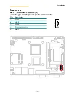
Page 25: ...in Description 1 2 3 4 5 1 12V 2 GND 3 on off 4 Brightness control 5 GND INV1 LCD Inverter Connector 8 PC17 PC1 S7 S1 1 2 1 72 74 71 73 204 203 7 1 1 2 17 15 18 16 51 52 4 2 3 1 4 1 2 9 10 1 3 1 2 9 1...

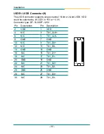
Page 26: ...onnector type DF 13 30DP 1 25V Pin Description Pin Description 1 29 30 2 2 VDD 1 VDD 4 N C 3 TX1_CLK 6 N C 5 TX1_CLK 8 GND 7 GND 10 N C 9 TX1_D0 12 N C 11 TX1_D0 14 GND 13 GND 16 N C 15 TX1_D1 18 N C...

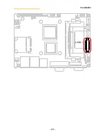
Page 27: ...23 Installation PC17 PC1 S7 S1 1 2 1 72 74 71 73 204 203 7 1 1 2 17 15 18 16 51 52 4 2 3 1 4 1 2 9 10 1 3 1 2 9 1 2 9 1 1 1 1 8 7 2 1 10 9 2 1 1 2 9 10 4 10 9 2 1 2 30 29 1 10 9 2 1 1 1 1 5 1 1 LVDS1...

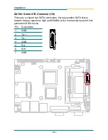
Page 28: ...twice the transfer speed of first generation SATA drives Pin Description 1 7 1 GND 2 TX 3 TX 4 GND 5 RX 6 RX 7 GND SATA1 Serial ATA Connector 10 PC17 PC1 S7 S1 1 2 1 72 74 71 73 204 203 1 2 17 15 18 1...

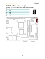
Page 29: ...nector Pin Description 1 2 3 4 1 5V 2 GND 3 GND 4 12V PWROUT1 SATA Power Connector 11 PC17 PC1 S7 S1 1 2 1 72 74 71 73 204 203 7 1 1 2 17 15 18 16 51 52 4 2 3 1 2 9 10 1 3 1 2 9 1 2 9 1 1 1 1 8 7 2 1...

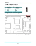
Page 30: ...2 4 2 3 1 4 1 2 9 10 1 3 1 2 9 1 2 9 1 1 1 1 8 7 2 1 10 9 2 1 1 2 9 10 4 10 9 2 1 2 30 29 1 10 9 2 1 1 1 1 5 1 1 AUDIO1 Connector type 2 00mm pitch 2x5 pin box header Pin Description Pin Description 1...

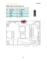
Page 31: ...10 9 1 2 1 DCD 2 2 RXD2 3 TXD2 4 DTR 2 5 GND 6 DSR 2 7 RTS 2 8 CTS 2 9 RI2 10 N C COM2 Serial Port Connector 13 PC17 PC1 S7 S1 1 2 1 72 74 71 73 204 203 7 1 1 2 17 15 18 16 51 52 4 2 3 1 4 1 2 9 10 1...

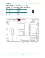
Page 32: ...422 RS 485 1 3 2 4 1 TX Data 2 TX Data 3 RX N C 4 RX N C JCOM1 COM2 RS 422 485 Connector 14 PC17 PC1 S7 S1 1 2 1 72 74 71 73 204 203 7 1 1 2 17 15 18 16 51 52 4 2 3 1 4 1 2 9 10 1 3 1 2 9 1 2 9 1 1 1...

Page 33: ...sfers at 1 5Mb s USB devices Connector type 2 00mm 2x5 pin headers Pin Description Pin Description 1 2 10 9 1 5V 2 5V 3 USBD 4 USBD 5 USBD 6 USBD 7 GND 8 GND 9 N C 10 N C Key USB1 2 USB Connectors 15...

Page 34: ...5 pin headers Pin Description Pin Description 10 9 1 2 1 DIO1 2 DIO2 3 DIO3 4 DIO4 5 DIO5 6 DIO6 7 DIO7 8 DIO8 9 5V 10 GND DIO1 Digital I O Connector 17 PC17 PC1 S7 S1 1 2 1 72 74 71 73 204 203 7 1 1...

Page 35: ...d is used to reboot the system POWER_LED Power LED Connector pin 3 4 This 2 pin connector connects to the case mounted power LED Power LED can be indicated when the CPU card is on or off And keyboard...

Page 36: ...32 Installation PC17 PC1 S7 S1 1 2 1 72 74 71 73 204 203 7 1 1 2 17 15 18 16 51 52 4 2 3 1 4 1 2 9 10 1 3 1 2 9 1 2 9 1 1 1 1 8 7 2 1 10 9 2 1 1 2 9 10 4 10 9 2 1 2 30 29 1 1 1 1 5 1 1 10 9 2 1 JFRT1...

Page 37: ...cription Pin Description 2 4 1 3 2 GND 4 12V 1 GND 3 12V 12VIN1 ATX 12V Connector 19 PC17 PC1 S7 S1 1 2 1 72 74 71 73 204 203 7 1 1 2 17 15 18 16 51 52 4 1 2 9 10 1 3 1 2 9 1 2 9 1 1 1 1 8 7 2 1 10 9...

Page 38: ...nector Pin Description 1 2 3 1 PS ON 2 GND 3 5V_SB EATX1 ATX Feature Connector 20 PC17 PC1 S7 S1 1 2 1 72 74 71 73 204 203 7 1 1 2 17 15 18 16 51 52 4 2 3 1 4 1 2 9 10 1 3 1 2 9 1 2 9 1 1 1 1 8 7 2 1...

Page 39: ...7 15 18 16 51 52 MC1 Mini card Socket 21 PC17 PC1 S7 S1 1 2 1 72 74 71 73 204 203 7 1 1 2 17 15 18 16 51 52 4 2 3 1 4 1 2 9 10 1 3 1 2 9 1 2 9 1 1 1 1 8 7 2 1 10 9 2 1 1 2 9 10 4 10 9 2 1 2 30 29 1 10...

Page 40: ...be a 12V fan Pin Description 1 2 3 1 GND 2 12V 3 FAN Speed FAN1 CPU Fan Connector 22 PC17 PC1 S7 S1 1 2 1 72 74 71 73 204 203 7 1 1 2 17 15 18 16 51 52 4 2 3 1 4 1 2 9 10 1 3 1 2 9 1 2 9 1 1 1 1 8 7...

Page 41: ...gabit Ethernet LAN1 2 Gigabit Ethernet Connectors 23 24 PC17 PC1 S7 S1 1 2 1 72 74 71 73 204 203 7 1 1 2 17 15 18 16 51 52 4 2 3 1 4 1 2 9 10 1 3 1 2 9 1 2 9 1 1 1 1 8 7 2 1 10 9 2 1 1 2 9 10 4 10 9 2...

Page 42: ...ouble stack USB type A USB3 USB Port Connectors 25 PC17 PC1 S7 S1 1 2 1 72 74 71 73 204 203 7 1 1 2 17 15 18 16 51 52 4 2 3 1 4 1 2 9 10 1 3 1 2 9 1 2 9 1 1 1 1 8 7 2 1 10 9 2 1 1 2 9 10 4 10 9 2 1 2...

Page 43: ...DATA0 3 DATA 2 4 SHIELD 11 DATA 1 3 SHIELD 19 DATA 0 5 SHIELD 4 DATA 4 LINK 1 NC 12 DATA 3 LINK 1 NC 20 DATA 5 LINK 1 NC 5 DATA 4 LINK 1 NC 13 DATA 3 LINK 1 NC 21 DATA 5 LINK 1 NC 6 DDC_CLK 14 5V 22...

Page 44: ...40 Installation PC17 PC1 S7 S1 1 2 1 72 74 71 73 204 203 7 1 1 2 17 15 18 16 51 52 4 2 3 1 4 1 2 9 10 1 3 1 2 9 1 2 9 1 1 1 1 8 7 2 1 10 9 2 1 1 2 9 10 4 10 9 2 1 2 30 29 1 10 9 2 1 1 1 1 5 1 1 DVI1...

Page 45: ...9 6 1 DCD 1 6 DSR 1 2 RXD1 7 RTS 1 3 TXD1 8 CTS 1 4 DTR 1 9 RI1 5 GND COM1 Serial Port Connector 27 PC17 PC1 S7 S1 1 2 1 72 74 71 73 204 203 7 1 1 2 17 15 18 16 51 52 4 2 3 1 4 1 2 9 10 1 3 1 2 9 1 2...

Page 46: ...1 S7 S1 PC17 S1 SGND1 S2 TXP S3 TXN S4 SGND2 S5 RXN S6 RXP S7 SGND PC1 CDI PC2 GND PC3 TBD PC4 TBD PC5 TBD PC6 TBD PC7 GND PC8 LED1 PC9 LED2 PC10 IO1 PC11 IO2 PC12 IO3 PC13 3 3V PC14 3 3V PC15 GND PC1...

Page 47: ...allation PC17 PC1 S7 S1 1 2 1 72 74 71 73 204 203 7 1 1 2 17 15 18 16 51 52 4 2 3 1 4 1 2 9 10 1 3 1 2 9 1 2 9 1 1 1 1 8 7 2 1 10 9 2 1 1 2 9 10 4 10 9 2 1 2 30 29 1 10 9 2 1 1 1 1 5 1 1 CFast1 on bot...

Page 48: ...44 Installation 2 3 The Installation Paths of CD Driver Windows 7 Driver Path CHIPSET EmETXe i250x CHIPSET WIN7 VGA EmETXe i250x GRAPHICS AUDIO EmETXe i250x AUDIO LAN EmETXe i250x ETHERNET...

Page 49: ...45 BIOS 3 Chapter 3 BIOS Chapter 3 BIOS...

Page 50: ...match what you see on your screen 3 1 BIOS Main Setup BIOS Information Display the BIOS information System Date Set the system date Note that the Day automatically changes when you set the date The da...

Page 51: ...elp F1 Save Exit Setup F10 Exit ESC Select Screen Select Enter Optimized Defaults F9 Launch PXE OpROM Launch Storage OpROM ACPI Settings IDE Configuration Disabled Enabled Devices with Option ROM F818...

Page 52: ...ACPI Auto Configuration Enable Hibernation ACPI Sleep State Disabled Enabled S1 CPU Stop Clock 3 2 1 ACPI Settings Enable Hibernation Enable or disable System ability to Hibernation OS S4 Sleep State...

Page 53: ...lasses of malicious buffer overflow Version 2 14 1219 Copyritght C 2011 American Megatrends Inc Advanced Aptio Setup Utility Copyright C 2011 American Megatrends Inc Select Item Change Opt Previous Va...

Page 54: ...ce Names if Present and Enabled Version 2 14 1219 Copyritght C 2011 American Megatrends Inc Advanced Aptio Setup Utility Copyright C 2011 American Megatrends Inc Select Item Change Opt Previous Values...

Page 55: ...workaround for OSes without EHCI hand off support Version 2 14 1219 Copyritght C 2011 American Megatrends Inc Advanced Aptio Setup Utility Copyright C 2011 American Megatrends Inc Select Item Change...

Page 56: ...ight C 2011 American Megatrends Inc Select Item Change Opt Previous Values F2 General Help F1 Save Exit Setup F10 Exit ESC Select Screen Select Enter Optimized Defaults F9 CPU temperature1 System temp...

Page 57: ...anced Aptio Setup Utility Copyright C 2011 American Megatrends Inc Select Item Change Opt Previous Values F2 General Help F1 Save Exit Setup F10 Exit ESC Select Screen Select Enter Optimized Defaults...

Page 58: ...erial Port Device Settings Change Settings Auto Enabled IO 3F8h IRQ 4 Enable or Disable Serial Port COM Serial Port 1 2 Configuration Serial Port Use the Serial port option to enable or disable the se...

Page 59: ...Save Exit Aptio Setup Utility Copyright C 2011 American Megatrends Inc Main Select Item Change Opt Previous Values F2 General Help F1 Save Exit Setup F10 Exit ESC Select Screen Select Enter Optimized...

Page 60: ...hipset Aptio Setup Utility Copyright C 2011 American Megatrends Inc Select Item Change Opt Previous Values F2 General Help F1 Save Exit Setup F10 Exit ESC Select Screen Select Enter Optimized Defaults...

Page 61: ...d during POST This has no effect if external graphics present IFGX Boot Type Select the Video Device which Version 2 14 1219 Copyritght C 2011 American Megatrends Inc Chipset Aptio Setup Utility Copyr...

Page 62: ...Exit Setup F10 Exit ESC Select Screen Select Enter Optimized Defaults F9 High Precision Event Timer Configuration High Precision Timer SLP_S4 Assertion Width Enabled 1 2 Seconds width of the SLP_S4 s...

Page 63: ...Hard Drive BBS Priorities 3 4 Boot Settings The Boot menu items allow you to change the system boot options Quiet Boot This allows you to select the screen display when the system boots Boot Configur...

Page 64: ...e Administrator rights 20 Maximum length Administrator Password HDD Security Configuration HDD 0 GLS85LS1008A Administrator Password Use the Administrator Password to set or change a administrator pas...

Page 65: ...your system is rebooted This would prevent unauthorized use of your computer You can determine when the password is required within the BIOS Features Setup Menu and its Security option If the Security...

Page 66: ...ions includes a list of tokens each of them corresponding to one device within the boot order Select a drive to immediately boot that device regardless of the current boot order Restore system to fact...

Page 67: ...xecution up to and including memory detection 0x30 0x4F PEI execution after memory detection 0x50 0x5F PEI errors 0x60 0x8F DXE execution up to BDS 0x90 0xCF BDS execution 0xD0 0xDF DXE errors 0xE0 0x...

Page 68: ...ding 0x05 OEM initialization before microcode loading 0x06 Microcode loading 0x07 AP initialization after microcode loading 0x08 North Bridge initialization after microcode loading 0x09 South Bridge i...

Page 69: ...nitialization North Bridge module specific 0x19 Pre memory South Bridge initialization is started 0x1A Pre memory South Bridge initialization South Bridge module specific 0x1B Pre memory South Bridge...

Page 70: ...Memory North Bridge initialization North Bridge module specific 0x3B Post Memory South Bridge initialization is started 0x3C Post Memory South Bridge initialization South Bridge module specific 0x3D P...

Page 71: ...0xE2 Video repost 0xE3 OS S3 wake vector call 0xE4 0xE7 Reserved for future AMI progress codes S3 Resume Error Codes 0xE8 S3 Resume Failed 0xE9 S3 Resume PPI not Found 0xEA S3 Resume Boot Script Error...

Page 72: ...x68 PCI host bridge initialization 0x69 North Bridge DXE initialization is started 0x6A North Bridge DXE SMM initialization is started 0x6B North Bridge DXE initialization North Bridge module specific...

Page 73: ...M DXE initialization codes 0x90 Boot Device Selection BDS phase is started 0x91 Driver connecting is started 0x92 PCI Bus initialization is started 0x93 PCI Bus Hot Plug Controller Initialization 0x94...

Page 74: ...0xB1 Runtime Set Virtual Address MAP End 0xB2 Legacy Option ROM Initialization 0xB3 System Reset 0xB4 USB hot plug 0xB5 PCI bus hot plug 0xB6 Clean up of NVRAM 0xB7 Configuration Reset reset of NVRAM...

Page 75: ...s entering S2 sleep state 0x03 System is entering S3 sleep state 0x04 System is entering S4 sleep state 0x05 System is entering S5 sleep state 0x10 System is waking up from the S1 sleep state 0x20 Sys...

Page 76: ...72 Appendix Appendix Appendix...

Page 77: ...er 0x000000C0 0x000000DF Direct memory access controller 0x00000020 0x00000021 Programmable interrupt controller 0x00000024 0x00000025 Programmable interrupt controller 0x00000028 0x00000029 Programma...

Page 78: ...ces 0x00000080 0x00000080 Motherboard resources 0x00000092 0x00000092 Motherboard resources 0x000000B2 0x000000B3 Motherboard resources 0x00000680 0x0000069F Motherboard resources 0x00001000 0x0000100...

Page 79: ...0FF Numeric data processor 0x0000F130 0x0000F137 Standard Dual Channel PCI IDE Controller 0x0000F120 0x0000F123 Standard Dual Channel PCI IDE Controller 0x0000F110 0x0000F117 Standard Dual Channel PCI...

Page 80: ...PCI standard PCI to PCI bridge IRQ 11 Video Controller VGA Compatible IRQ 11 PCI PCI Simple Communications Controller IRQ 5 Ethernet Controller IRQ 5 SM Bus Controller IRQ 22 Microsoft UAA Bus Driver...

Page 81: ...ns Controller 0xF7C00000 0xF7C1FFFF Ethernet Ethernet Controller 0xF7C28000 0xF7C28FFF Ethernet Ethernet Controller 0xF7C27000 0xF7C273FF Standard Enhanced PCI to USB Host Con troller 0xF7C20000 0xF7C...

Page 82: ...FFFFF Motherboard resources 0xFED20000 0xFED3FFFF Motherboard resources 0xFED90000 0xFED93FFF Motherboard resources 0xFED45000 0xFED8FFFF Motherboard resources 0xFEE00000 0xFEEFFFFF Motherboard resour...

Page 83: ...0x07 bool __fastcall TForm1 Check_ID void DWORD iData SetPortVal SIO_INDEX SIO_EN 1 SIO Enable SetPortVal SIO_INDEX SIO_EN 1 SetPortVal SIO_INDEX SIO_EN 1 SetPortVal SIO_INDEX 0x01 1 SetPortVal SIO_IN...

Page 84: ...ble SetPortVal SIO_INDEX SIO_EN 1 SetPortVal SIO_INDEX SIO_EN 1 LDN GPIO SetPortVal SIO_INDEX LDN_ADDR 1 SetPortVal SIO_DATA 0x06 1 GPIO5 Mode SetPortVal SIO_INDEX 0xA0 1 SetPortVal SIO_DATA oMode 1 G...

Page 85: ...F0 0xF0 unsigned char oDataL 8 0xF7 0xFD 0xFE 0xFB 0xEF 0xDF 0xBF 0x7F unsigned char oDataH 8 0xF8 0xF2 0xF1 0xF4 0x1F 0x2F 0x4F 0x8F unsigned char iData 8 0x10 0x20 0x40 0x80 0x08 0x02 0x01 0x04 InDa...

Page 86: ...e table Super IO chipaset Fintek F81866D Pin Description Chipset Pin Chipset Pin description 1 DIO1 9 GPIO50 2 DIO2 10 GPIO51 3 DIO3 11 GPIO52 4 DIO4 12 GPIO53 5 DIO5 13 GPIO54 6 DIO6 14 GPIO55 7 DIO7...

Reviews: