EK49
2
EK49U Rev A
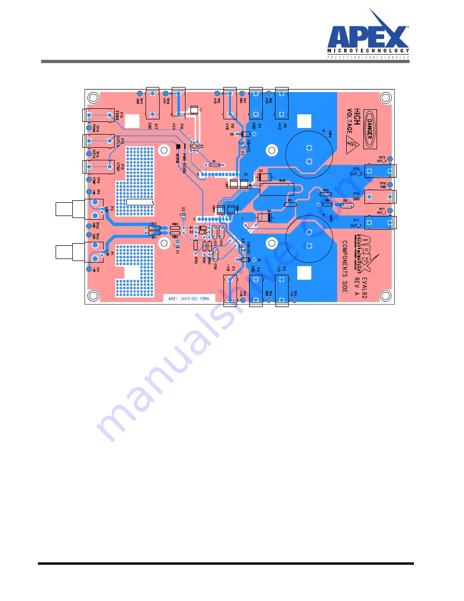
Figure 2: Circuit Board Layout
Page 1: ...t Configure Diagram OUT_2 GND IN OUT_1 VTMP PDWN OCFLG IN OUT MP165KL 16 15 14 13 12 11 10 9 8 7 6 5 4 3 2 1 17 18 19 20 N C N C N C VB VS GND VS VB GND VS ILIM VB CC2 CC1 IN IN VTMP VS VB OCFLG ILIM...
Page 2: ...EK49 2 EK49U Rev A Figure 2 Circuit Board Layout...
Page 3: ...CBP1 CBP3 CBP4 CBP6 C5750X7R2E105K230KA 1 F 250V Film Cap 5 CBP2 CBP5 KMH450VN471M35X50T2 470 F 450V Electrolytic Cap 2 CC1 CC2 561R10TCCV33BA 3 3pF 1kV Ceramic Cap 2 Hardware HS31 Heatsink for Amplif...
Page 4: ...BP5 on the component side of the board Ensure that the orienta tion of the components match the circuit schematic drawing 8 Mount the BNC connector provided with the kit 146510CJ and solder it to the...
Page 5: ...gure 3 Evaluation Kit Assembly Top View Figure 4 Evaluation Kit Assembly Bottom View 1 2 1 23 x MS11 Cage Jacks 2 2 x 4 Screw Pan Head 1 2 3 4 1 4 x 8 0 375 Screw 2 4 x Spacer Grommets 3 4 x 8 0 98 Sc...
Page 6: ...he DUT side to ensure that there is no short and to check if all the pins cage jacks read cor rect voltages Now mount the MP165 on EVAL 92 If connecting a resistor load connect between ports P11 and P...
Page 7: ...EK49 EK49U Rev A 7 Figure 5 Normal Operation Figure 6 Current Limit Operation...
Page 8: ...information Apex Microtechnology grants no license expressed or implied under any patents mask work rights copyrights trademarks trade secrets or other intellectual property rights Apex Microtechnolo...