EK37
2
EK37U Rev A
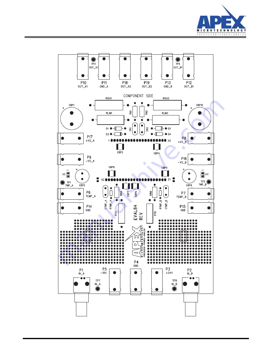
Figure 2: EVAL 76 PCB Layout
Page 1: ...he connectors at the edges of the circuit The circuit provides a line termination of 50 Figure 1 EK37 Schematic 1 2 3 4 5 6 7 8 9 10 11 12 13 14 15 16 31 30 29 28 27 25 24 23 22 21 20 19 18 17 32 26 3...
Page 2: ...EK37 2 EK37U Rev A Figure 2 EVAL 76 PCB Layout...
Page 3: ...0V 2 CBP1 CBP10 LGU2D221MELY Alum 220uF 200V 2 CBP3 CBP4 C5750X7R2E105K230KA Film 1uf 250V 2 CBP5 CBP6 C5750X7R2E105K230KA Film 1uf 250V 2 CBP7 CBP8 C5750X7R2E105K230KA Film 1uf 250V 2 Diodes D1 D2 D3...
Page 4: ...board Also mount the banana jacks on the board Install other miscellaneous components like jumpers and test points to com plete your application circuit 8 From the DUT side of the PCB snap the spacer...
Page 5: ...EK37 EK37U Rev A 5 Figure 3 Top View 1 2 3 4 5 1 4 X 8 X 0 375 SCREW 2 4 X 8 X 2 00 HEX STANDOFFS 3 4 X 4 X 0 187 SCREW 4 4 X SPACER GROMMETS 5 4 X 8 X 0 625 SCREW...
Page 6: ...EK37 6 EK37U Rev A Figure 4 Bottom View...
Page 7: ...Input and output waveforms can be checked on an Oscillo scope by connecting it to the test points mounted on the board Begin the test with minimum values of input and supply voltage Volt meters can b...
Page 8: ...n Apex Microtechnology grants no license expressed or implied under any patents mask work rights copyrights trademarks trade secrets or other intellectual property rights Apex Microtechnology owns the...