A1101R09x – Users Manual
Page 9 of 26
Release Date 02/10/11
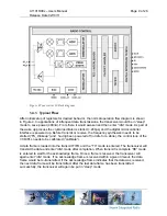
Figure 3 Transceiver IC block diagram.
1.4.1. Typical Flow
After initial setup of registers for desired behavior, the normal operation flow diagram is shown
in Figure 4. In applications of infrequent data transmissions, the transceiver would be in “sleep”
mode to save power (400nA). From there it would awaken and then enter “idle” mode. As part of
the wake up process the crystal oscillator is started (~240µs) and the digital microcontroller
interface is powered up. Before transmit or receive, the frequency synthesizer needs to be
started (“FS_Wakeup”) and, having been powered off (or idle for a while), the control loop of the
VCO/PLL needs to be calibrated (“calibrate”).
A data frame is loaded into the transmit FIFO and the “TX” mode is entered. The transceiver will
transmit the data and enter “idle” mode after completion. When transmit is complete “RX” mode
is entered to wait for the acknowledge frame. Once a frame is received, the transceiver will
again enter “idle” mode. If no acknowledge frame is received within a given timeout, the data
frame would be re-transmitted. If the acknowledge frame indicates that the data was received,
the next data frame will be transmitted. After the last data frame has been transmitted
successfully, the transceiver will again be put in “sleep” mode.


