UG-547
Evaluation Board User Guide
Rev. 0 | Page 4 of 8
2-pin header to allow adjacent channels to temporarily be
shorted together.
7.
A 0805 pad layout between the signal and ground where a
load capacitor or resistor can be installed.
8.
Pads to the adjacent channels are provided to allow permanent
connection of adjacent channels. Inputs can be fanned out
to several channels, or inputs and outputs can be connected
together to allow signals to loopback.
Figure 2 shows many of the optional components installed, as well
as how jumpers can be used to temporarily connect channels.
This figure shows a signal connected to the first channel SMA
and then fanned out to the top three channels and monitored by
an active scope probe.
BYPASS ON THE PCB
Several positions and structures are provided to allow optimum
bypass of the evaluation board. Provision has been made for
optional surface-mount bulk capacitors to be installed near the
power connectors to compensate for long cables to the power
supply. Parallel bypass capacitors are installed near the
ADuM7643
and consist of a 0.1 µF capacitor for each V
DDxA
on the top side
and bottom side and a 0.1 µF capacitor for each V
DDxB
on the
bottom side of the board. It is best to use the top side bypass
positions if possible.
The PCB also implements a distributed capacitive bypass on the
PCB. This consists of power and ground planes closely spaced
on the inner layers of the PCB. This minimizes noise and the
transmission of EMI without using complex design features.
HIGH VOLTAGE CAPABILITY
This PCB is designed in adherence with 2500 V basic insulation
practices. High voltage testing beyond 2500 V is not recommended.
Appropriate care must be taken when using this evaluation board
at high voltages, and the PCB should not be relied on for safety
functions because it has not been high potential tested (also
known as hipot tested or dielectric withstanding voltage tested)
or certified for safety.
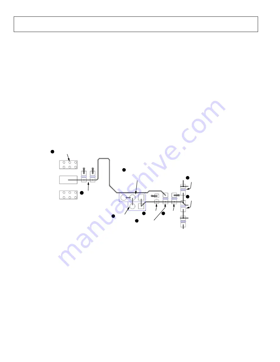
11405-
004
1
SMA CONNECTOR PADS
2
TERMINATION
2 × 100Ω
5
2-PIN HEADER
GND/SIGNAL
4
PULL-UP
PAD
7
PULL-DOWN
PAD
3
CONNECT
TO SMA
8
CONNECT TO
NEXT CHANNEL UP
8
CONNECT TO
NEXT CHANNEL DOWN
6
OPEN HOLES FOR
SOLDERED WIRES OR 200mil
TEKTRONIX HEADER,
GND/GND/SIGNAL
NOTES
1. THE NUMBERED COMPONENTS IN THIS FIGURE CORRESPOND
TO THE DESCRIPTIONS IN THE DATA I/O STRUCTURES SECTION.
Figure 3. Configuration and Monitoring Structures (Showing a Datapath from an External Connection to the DUT Pin)


