UG-1926
Rev. 0 | Page 4 of 20
EVALUATION BOARD HARDWARE
POWER SUPPLIES AND DEFAULT LINK OPTIONS
The EVAL-ADUCM420QSP1Z development system can be
powered with the following options: a 5 V terminal block from
bench supplies, a 9 V wall mounted adapter, or a USB supply.
See Table 1 for the on-board jumper configurations for each
power supply option and other optional connectors. Locate
Pin 1 for each header pin for the supply.
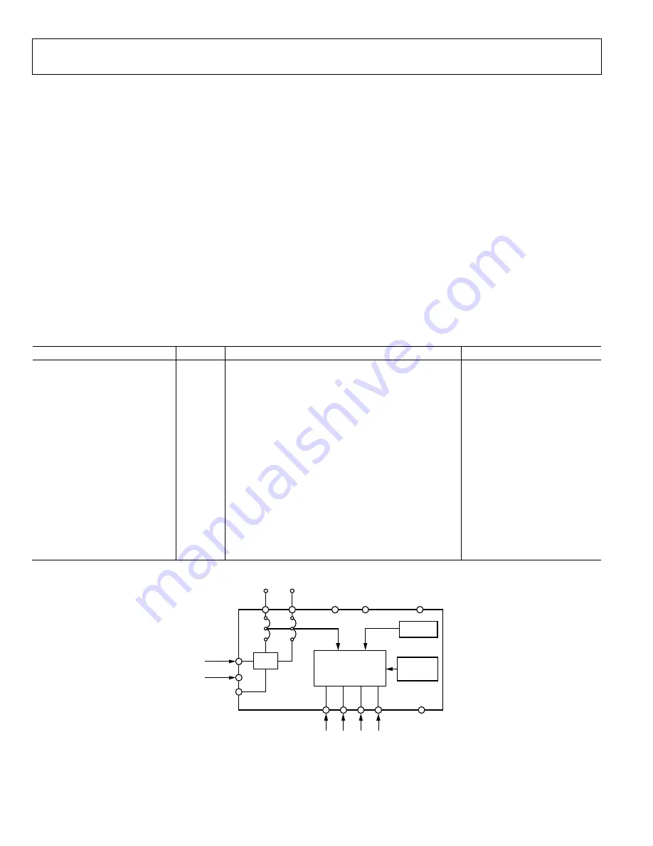
For any of the power supply options, place the jumpers shown
in Table 1 in the required operating setup before supplying
power to the EVAL-ADUCM420QSP1Z (see Figure 2).
Each power supply is decoupled to the relevant ground plane
with 10 µF and 0.1 µF capacitors. Each device supply pin is also
decoupled with a 10 µF and 0.1 µF capacitor pair to the relevant
ground plane.
EVAL-ADUCM420QSP1Z Board Interface
has on-chip digital peripheral interfaces, such
as a universal asynchronous receiver/transmitter (UART), serial
peripheral interface (SPI), management data input/output
(MDIO), and I
2
C. See Figure 1 for the on-board component
locations.
Bench Power Supply Option
The ADuCM420 requires 5 V for normal operation. Replicating
the jumper configuration in Table 1, the 5 V terminal block
supply passes through LDO regulators to regulate the power
supply. The ADuCM420 can also configure the IOVDD1 and
DVDD power supplies to be 1.2 V or 1.8 V, and 1.8 V or 3.3 V,
respectively. To configure these supply options, select the
required position on Jumper P11 for IOVDD1 and Jumper P15
for DVDD. P11 and P15 are on the solder side (bottom side of
the evaluation board.)
Table 1. Jumper Configurations for the EVAL-ADUCM420QSP1Z
Jumper No.
Optional Jumper Configuration
Bench Supply or 9 V Wall Wart
JP6—Future Technology Devices
International (FTDI) Supply
No
Short.
Yes
JP7—USB
Yes
Short.
Yes
P11—IOVDD1
No
Pin 1 and Pin 2 = 1.8 V, Pin 2 and Pin 3 = 1.2 V.
Yes
P15—DVDD
No
Pin 1 and Pin 2 = 3.3 V, Pin 2 and Pin 3 = 1.8 V.
Yes
P7—SIN1 Level Shifter
Yes
Pin 1 and Pin 2 = IOVDD0, Pin 2 and Pin 3 = IOVDD1.
Yes
P12—SOUT1 Level Shifter
Yes
Pin 1 and Pin 2 = IOVDD0, Pin 2 and Pin 3 = IOVDD1.
Yes
P14—LED Display
Yes
Short.
Yes
P5—IOVDD0 Pull-Up
Yes
Short.
Yes
JP1—SWCLK Pull-Up
Yes
JP3, JP4, and JP5 are optional pull-ups. The R14 resistor
(see Figure 1) must be populated with values that are at
least 100 kΩ to use these optional pull-ups.
Yes
JP2—SWDIO Pull-Up
Yes
Short.
Yes
JP3—P2.2 or SWO Pull-Up
Yes
Short.
Yes
JP8 to JP10
Yes
These pins use the on-board FTDI chip that can be used
on the I
2
C downloader.
Yes
+1.2V
P11
B
A
B
A
+5V
DGND
LDOs
P15
+1.8V
UART
ADuCM420
IOVDD1
USB/WALL WART
mIDAS-Link
AGND
SPI
SPI
IOGND
IOGND
IOGND
J-LINK
I
2
C
25844-
006
Figure 2. On-Board Jumper Configuration Diagram


