Analog Devices EVAL-ADGS1612SDZ User Manual Download Page 5

EVAL-ADGS1612SDZ 

User Guide 

UG-1199


Rev. 0 | Page 5 of 11 

EVALUATION BOARD SOFTWARE 

INSTALLING THE SOFTWARE 

The EVAL-ADGS1612SDZ evaluation board uses the Analog 
Device

Analysis Control Evaluation (ACE)

 software

ACE

 is a 

desktop software application that allows the evaluation and 
control of multiple evaluation systems. 

The 

ACE

 installer installs the necessary SDP drivers and .NET 

Framework 4 by default. Install 

ACE

 before connecting the SDP. 

The 

ACE

 software and access to full instructions on how to 

install and us

ACE

 can be found on the Analog Devices 

website. 

After the installation is finished, the EVAL-ADGS1612SDZ 
evaluation board plug-ins appear when openin

ACE

.  

INITIAL SET UP 

To set up the evaluation board, complete the following steps: 

1.


Connect the evaluation board to the SDP board and 
connect the SDP board to the computer via a USB cable. 

2.


Power the evaluation board as described in the Power 
Supplies s
ection. 

3.


Run th

ACE

 application. The EVAL-ADGS1612SDZ 

board plug-ins appear in the attached hardware section of 
the 

Start

 tab. 

4.


Double-click on the evaluation board plug-in to open the 
evaluation board view seen in Figure 2. 

5.


The chip block diagram can be accessed by double-clicking 
on th

ADGS1612

 chip (see Figure 2). This view provides a 

basic representation of functionality of the evaluation board. 
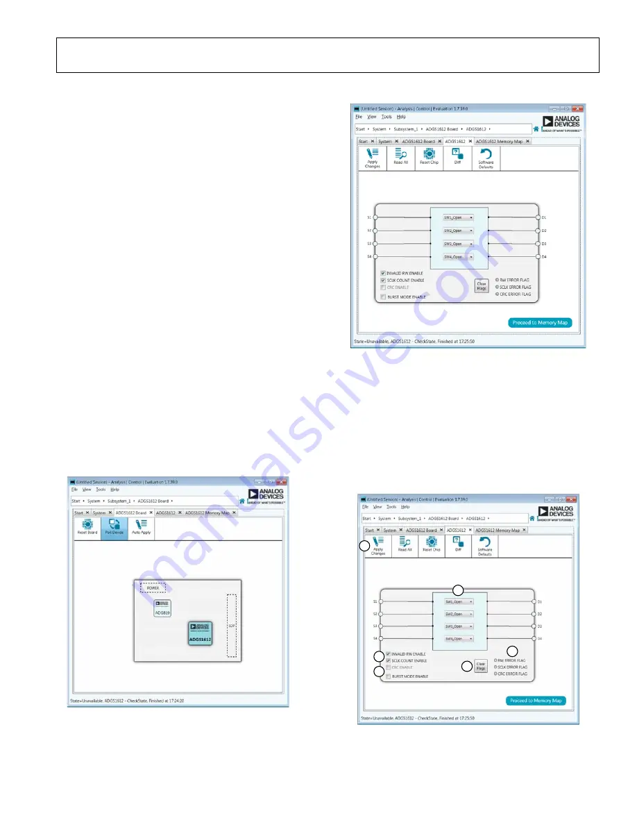
The main functions are labeled in Figure 3. 


Figure 2. Evaluation Board View of the EVAL-ADGS1612SDZ 


Figure 3. Chip Block Diagram View for th

ADGS1612


BLOCK DIAGRAM AND DESCRIPTION 

The EVAL-ADGS1612SDZ software is organized so that it 
appears similar to the functional block diagram shown in the 
data sheet. In this way, it is easy to correlate the functions on the 
EVAL-ADGS1612SDZ board with the full description of each 
block, register, and settings is given in th

ADGS1612

 data sheet. 

Some of the blocks and their functions are described here as they 
pertain to the evaluation board. The full screen block diagram, 
shown in Figure 4, describes the functionality of each block. 


Figure 4. EVAL-ADGS1612SDZ Block Diagram with Labels 


16

26

3-

00

2

16

263-

0

03

16

26

3-

0

04

F

B

A

E

D

C

Summary of Contents for EVAL-ADGS1612SDZ

Page 1: ...interface SPI The SPI has robust error detection features These are cyclic redundancy check CRC error detection invalid read write address detection and serial clock SCLK count error detection It is possible to daisy chain multiple ADGS1612 devices together This enables the configuration of multiple devices with a minimal amount of digital lines The ADGS1612 also supports burst mode that decreases...

Page 2: ...History 2 ADGS1612 Evaluation Board Layout 3 Evaluation Board Hardware 4 Power Supplies 4 Input Signals 4 Link Options 4 Evaluation Board Software 5 Installing the Software 5 Initial Set Up 5 Block Diagram And Description 5 Memory Map 6 Evaluation Board Schematics and Artwork 7 Ordering Information 11 Bill of Materials 11 REVISION HISTORY 1 2018 Revision 0 Initial Version ...

Page 3: ...EVAL ADGS1612SDZ User Guide UG 1199 Rev 0 Page 3 of 11 ADGS1612 EVALUATION BOARD LAYOUT Figure 1 16263 001 ...

Page 4: ...ads which can place a load on the signal path to ground A 0 Ω resistor is placed in the signal path and can be replaced with a user defined value The resistor combined with the 0603 pads can create a simple resistor capacitor RC filter LINK OPTIONS A number of link options are provided on the EVAL ADGS1612SDZ board that must be set for the required operating conditions before using Table 1 describ...

Page 5: ...ication The EVAL ADGS1612SDZ board plug ins appear in the attached hardware section of the Start tab 4 Double click on the evaluation board plug in to open the evaluation board view seen in Figure 2 5 The chip block diagram can be accessed by double clicking on the ADGS1612 chip see Figure 2 This view provides a basic representation of functionality of the evaluation board The main functions are l...

Page 6: ...values to the devices Memory Map All registers are fully accessible from the memory map tab this allows registers to be edited at a bit level see Figure 5 and Figure 6 The bits shaded in dark gray are read only bits and cannot be accessed from ACE all other bits are toggled The Apply Changes button transfers data to the device All changes here correspond to the block diagram for example if the int...

Page 7: ...EVAL ADGS1612SDZ User Guide UG 1199 Rev 0 Page 7 of 11 EVALUATION BOARD SCHEMATICS AND ARTWORK Figure 7 EVAL ADGS1612SDZ Schematic 1 Figure 8 EVAL ADGS1612SDZ Schematic 2 16263 007 16263 008 ...

Page 8: ...UG 1199 EVAL ADGS1612SDZ User Guide Rev 0 Page 8 of 11 Figure 9 EVAL ADGS1612SDZ Schematic 3 Figure 10 EVAL ADGS1612SDZ Silk Screen 16263 009 16263 010 ...

Page 9: ...EVAL ADGS1612SDZ User Guide UG 1199 Rev 0 Page 9 of 11 Figure 11 EVAL ADGS1612SDZ Top Layer Figure 12 EVAL ADGS1612SDZ Layer 2 16263 011 16263 012 ...

Page 10: ...UG 1199 EVAL ADGS1612SDZ User Guide Rev 0 Page 10 of 11 Figure 13 EVAL ADGS1612SDZ Layer 3 Figure 14 EVAL ADGS1612SDZ Bottom Layer 16263 013 16263 014 ...

Page 11: ...hirdParty includesanyentityother thanADI Customer their employees affiliatesandin houseconsultants TheEvaluationBoardisNOT soldtoCustomer allrightsnotexpresslygrantedherein including ownership of the Evaluation Board are reserved by ADI CONFIDENTIALITY This Agreement and the Evaluation Board shall all be considered the confidential and proprietary information of ADI Customer may not discloseor tra...

Reviews: