background image


EVAL-ADG788EBZ


Rev. 0 | Page 5 of 8 

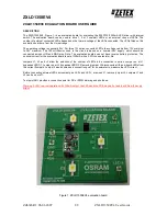
EVALUATION BOARD SCHEMATICS AND ARTWORK 


J4-1

J4-3

J4-2

T8

V

SS

V

DD

T9

T10

C3

10µF

C4

10µF

+

+

J23

3

2

1

AB

CASE
CASE

GND

TOP

BOTTOM

PHONO_DUAL

J1

1

4

5

2

3

CASE
CASE

GND

TOP

BOTTOM

PHONO_DUAL

J2

1

4

5

2

3

CASE
CASE

GND

TOP

BOTTOM

PHONO_DUAL

J3

1

4

5

2

3

CASE
CASE

GND

TOP

BOTTOM

PHONO_DUAL

J5

1

4

5

2

3

J9

3

2

V

DD

1

AB

J8

T6

8

9

10

7

6

5

4

3

2

1

IN2

IN3

NC

S2A

D2

S2B

GND

V

SS

V

SS

S1B

D1

S3B

D3

S3A

V

DD

S4B

D4

S4A

IN4

IN1

S1A

13

12

11

14

15

16

17

18

19

20

T7

3

2

V

DD

1

AB

U1

ADG788

T4

T5

T3

C1

0.1µF

T1

T2

T19

T18

T17

T16

T15

T14

V

DD

T13

T12

T11

C2

0.1µF

R4

50

R3

50

R1

10k

R2

10k

V

DD

J12

J13

3

2

1

AB

V

DD

3

2

1

AB

R5

10k

R6

10k

R7

50

R8

50

CASE

CASE

TOP

GND

BOTTOM

PHONO_DUAL

J11

3

2

3

2

2

2

4

5

1

CASE

CASE

TOP

GND

BOTTOM

PHONO_DUAL

J10

4

5

1

3

CASE

CASE

TOP

GND

BOTTOM

PHONO_DUAL

J7

4

5

1

3

CASE

CASE

TOP

GND

BOTTOM

PHONO_DUAL

J6

4

5

1

0

67

56

-00

2


Figure 2. Evaluation Board Schematic  


Summary of Contents for EVAL-ADG788EBZ

Page 1: ...s Inc All rights reserved FEATURES Supply voltage Single 1 8 V to 5 5 V Dual 2 5 V TTL CMOS compatible control inputs Switch control options On board links External control signals RoHS compliant GENERAL DESCRIPTION This data sheet describes the evaluation board for the ADG788 a triple SPDT switch packaged in a compact 4 mm 4 mm body 20 lead LFCSP package The switches are designed using an enhance...

Page 2: ...luation Board 1 Revision History 2 Evaluation Board Hardware 3 Power Supply 3 Switch Control 3 Connections and Test Points 4 Evaluation Board Schematics and Artwork 5 Ordering Information 7 Bill of Materials 7 Ordering Guide 7 ESD Caution 7 REVISION HISTORY 6 07 Revision 0 Initial Version ...

Page 3: ...OL The four input pins IN1 IN2 IN3 and IN4 control the opera tion of the ADG788 Link J8 Link J9 Link J12 and Link J13 control the logic levels applied to these pins and allow the user to drive these pins with external signals applied to Connector J5 and Connector J11 the signals have 50 Ω on board termination resistors to GND Table 2 describes the configuration achieved for each position of these ...

Page 4: ... S1B Bottom T3 S2B J3 Top T4 D2 Bottom T5 S2A J4 VDD T9 VDD GND T10 GND VSS T8 VSS J51 Top T6 IN2 Bottom T7 IN3 J6 Top T11 S3A Bottom T12 D3 J7 Top T13 S3B Bottom T14 S4B J10 Top T15 D4 Bottom T16 S4A J111 Top T17 IN4 Bottom T18 IN1 1 This connector is tied to the ADG788 pins only when Link J8 and Link J9 are set in Position B and J12 and J13 are in Position A ...

Page 5: ... 7 6 5 4 3 2 1 IN2 IN3 NC S2A D2 S2B GND VSS VSS S1B D1 S3B D3 S3A VDD S4B D4 S4A IN4 IN1 S1A 13 12 11 14 15 16 17 18 19 20 T7 3 2 VDD 1 A B U1 ADG788 T4 T5 T3 C1 0 1µF T1 T2 T19 T18 T17 T16 T15 T14 VDD T13 T12 T11 C2 0 1µF R4 50Ω R3 50Ω R1 10kΩ R2 10kΩ VDD J12 J13 3 2 1 A B VDD 3 2 1 A B R5 10kΩ R6 10kΩ R7 50Ω R8 50Ω CASE CASE TOP GND BOTTOM PHONO_DUAL J11 3 2 3 2 2 2 4 5 1 CASE CASE TOP GND BOTT...

Page 6: ...DG788EBZ Rev 0 Page 6 of 8 06756 003 06756 004 Figure 3 Component Side PCB Drawing Layer 1 Figure 4 Solder Side PCB Drawing Layer2 Component Side View 06756 005 Figure 5 Component Side Silkscreen PCB Drawing ...

Page 7: ...1 J2 J3 J5 J6 J7 J10 J11 Dual phono connector FEC 128 0670 1 J4 3 pin power block FEC 963 2980 5 J8 J9 J12 J13 J23 3 pin SIL header and shorting link FEC 486 1220 and FEC 148 029 4 R1 R2 R5 R6 10 kΩ SMD resistor FEC 933 0399 4 R3 R4 R7 R8 50 Ω SMD resistor FEC 933 1336 19 T1 to T19 Test point FEC 873 1128 1 U1 ADG788BCPZ Analog Devices Inc ORDERING GUIDE Model Package Description EVAL ADG788EBZ1 A...

Page 8: ...EVAL ADG788EBZ Rev 0 Page 8 of 8 NOTES 2007 Analog Devices Inc All rights reserved Trademarks and registered trademarks are the property of their respective owners EB06756 0 6 07 0 ...

Reviews: