background image

EVAL-AD5341DBZ User Guide 

UG-982 


Rev. 0 | Page 5 of 12 

14517-

004


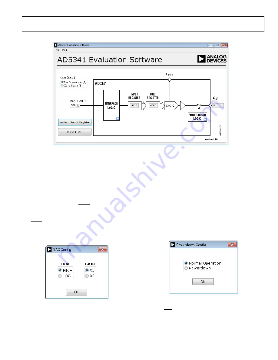
Figure 4

AD5341

 Evaluation Board Software Main Window  


SOFTWARE OPERATION 

The software for the 

AD5341

 allows users to program values to 

the input and DAC registers of the DAC. 

Write to Input Register 

Click 

Write to Input Register

 to load the code of the input data 

control to the input register of the DAC. 

LDAC Control 

Click 

Pulse LDAC

 to bring the LDAC pin low and then back to 

high, which copies the data from the input registers to the DAC 
registers, and the outputs update accordingly. Alternatively, set 
the LDAC pin high or low by clicking the blue progressive 
disclosure button in the 

INTERFACE LOGIC

 block. A window 

then opens that allows the user to click the appropriate 

LDAC


setting, as shown in Figure 5. 

14517-

005


Figure 5. 

DAC Config

 Window 


GAIN Control 

Set the GAIN pin high or low by clicking the blue progressive 
disclosure button in the 

INTERFACE LOGIC

 block. A window 

then opens that allows the user to click the appropriate 

GAIN


setting, as shown in Figure 5. Click 

GAIN X1

 to set a full-scale 

output of 2.5 V or click 

GAIN X2

 to set a full-scale output of 5 V. 

Power-Down Control 

Click the blue progressive disclosure button in the 

POWER-

DOWN LOGIC

 block to access a selection box that allows the 

device to operate in normal mode or power-down mode. A 
window then opens that allows the user to click the power-
down setting for the DAC, as shown in Figure 6. Click 

OK

 to 

write the appropriate values to th

AD5341

 when the power-

down settings for the DAC are selected. 

14517-

006


Figure 6. 

Powerdown Config

 Window 

CLR Control 

Set the CLR pin high or low using LK2 as described in the 
Daughter Board Link Options section and Table 3. Click the 
appropriate 

CLR (LK2)

 setting on the GUI to match the 

daughter board setting (see Figure 4)


Summary of Contents for EVAL-AD5341DBZ

Page 1: ...on software HARDWARE REQUIRED EVAL SDP CB1Z controller board SDP B controller board must be purchased separately GENERAL DESCRIPTION This user guide details the operation of the evaluation board for the AD5341 single channel voltage output DAC The EVAL AD5341DBZ evaluation board helps users quickly prototype new AD5341 circuits and reduce design times The AD5341 operates from a single 2 5 V to 5 5...

Page 2: ...sion History 2 Evaluation Board Hardware 3 Power Supplies 3 Link Options 3 Daughter Board Link Options 3 Evaluation Board Software Quick Start Procedures 4 Installing the Software 4 Running the Software 4 Software Operation 5 Evaluation Board Schematics and Artwork 6 EVAL MBnanoDAC SDZ Motherboard 6 EVAL AD5341DBZ Daughter Board 9 Ordering Information 11 Bill of Materials 11 REVISION HISTORY 2 201...

Page 3: ...3V3 LK7 B DAUGHTER BOARD LINK OPTIONS The EVAL AD5341DBZ daughter board has two link options The links control the settings for the reference BUF and CLR pins Table 3 shows how the links are configured Table 3 Link Options for Daughter Board Link Number Pin Position LK1 BUF A unbuffered default B buffered LK2 CLR A no operation default B zero scale Table 4 Link Functions Link Number Function REF1 ...

Page 4: ... USB cable included in the evaluation kit 6 Proceed through any dialog boxes that appear to finalize the installation when the software detects the EVAL AD5341DBZ RUNNING THE SOFTWARE To run the EVAL AD5341DBZ software take the following steps 1 Connect the EVAL AD5341DBZ to the SDP B and connect the USB cable between the SDP B and the PC 2 Power up the EVAL AD5341DBZ as described in the Power Sup...

Page 5: ...nfig Window GAIN Control Set the GAIN pin high or low by clicking the blue progressive disclosure button in the INTERFACE LOGIC block A window then opens that allows the user to click the appropriate GAIN setting as shown in Figure 5 Click GAIN X1 to set a full scale output of 2 5 V or click GAIN X2 to set a full scale output of 5 V Power Down Control Click the blue progressive disclosure button i...

Page 6: ...9 PAR_D3 18 PAR_D5 17 GND 16 PAR_D7 15 PAR_D9 14 PAR_D11 13 PAR_D13 12 PAR_D14 11 GND 10 PAR_D17 9 PAR_D19 8 PAR_D21 7 PAR_D23 6 GND 5 USB_VBUS 4 GND 3 GND 2 NC 1 VIN J10 1 A0 2 A1 3 A2 4 VSS 8 VCC 7 WP 6 SCL 5 SDA U3 24LC32 R2 100kΩ R4 DNP R3 100kΩ DGND AGND L1 BEAD R1 1 6Ω C11 4 7µF C10 0 1µF C7 10µF 1 IN 2 GND 3 EN 4 NC 5 OUT U2 ADP121 AUJZ33 C3 1µF C4 1µF C B A LK5 J6 1 J6 2 C5 0 1µF C6 10µF A...

Page 7: ...2 DB3 VOUT_0 VOUT_1 VOUT_2 VOUT_3 VOUT_4 VOUT_5 VOUT_6 VOUT_7 SCL SDA DGND VLOGIC SCL SDA DGND VLOGIC SYNC SDO SDIN SCLK DGND VLOGIC PD GAIN DGND LDAC CLR VLOGIC DGND CS WR DB11 DB5 DB10 DB4 AGND Figure 9 EVAL MBnanoDAC SDZ Motherboard Connectors to Daughter Board and Serial Interface 14517 010 VOUT_0 VOUT_1 VOUT_2 VOUT_3 VOUT_4 VOUT_5 VOUT_6 VOUT_7 3 2 1 U10 A AD8608ARUZ 5 6 7 U10 B AD8608ARUZ 10...

Page 8: ...UG 982 EVAL AD5341DBZ User Guide Rev 0 Page 8 of 12 14517 011 Figure 11 EVAL MBnanoDAC SDZ Motherboard Component Placement 14517 012 Figure 12 EVAL MBnanoDAC SDZ Motherboard Top Side Routing ...

Page 9: ...UT C1 DNP B A LK1 B A LK2 C2 0 1µF C3 10µF 1 3 5 7 9 2 4 6 8 10 J2 J3 1 J3 2 J3 3 J3 4 J3 5 J3 6 J4 1 J4 2 J4 3 J4 4 J4 5 J4 6 J4 7 J4 8 1 2 3 4 5 6 7 8 9 10 11 12 13 14 15 16 J1 VDD AGND VOUT_0 VLOGIC VLOGIC VDD VREF1 VREF2 VREF3 VREF4 VLOGIC SDA SCL SYNC SCLK SDO SDIN LDAC CLR PD GAIN VOUT_0 VOUT_1 VOUT_2 VOUT_3 VOUT_4 VOUT_5 VOUT_6 VOUT_7 DB6 DB7 DB8 DB9 DB0 DB1 DB2 DB3 DGND CS WR DB11 DB5 DB10...

Page 10: ...ide Rev 0 Page 10 of 12 14517 015 Figure 15 EVAL AD5341DBZ Daughter Board Component Placement 14517 016 Figure 16 EVAL AD5341DBZ Daughter Board Top Side Routing 14517 017 Figure 17 EVAL AD5341DBZ Daughter Board Bottom Side Routing ...

Page 11: ... way FEC 1667509 1 J10 120 way connector FEC 1324660 1 L1 Inductor SMD 600 Ω FEC 9526862 1 LK5 6 pin 3 2 0 1 inch header and shorting block FEC 148 535 and 150 411 36 pin strip 2 LK6 LK7 4 pin 2 2 0 1 inch headers and shorting blocks FEC 148 535 and 150 411 36 pin strip 4 REF1 REF2 REF3 REF4 10 pin 5 2 0 1 inch headers and shorting blocks FEC 1022227 and 150 411 1 R1 Resistor surge 1 6 Ω 1 0603 FE...

Page 12: ... Board As used herein the term Third Party includes any entity other than ADI Customer their employees affiliates and in house consultants The Evaluation Board is NOT sold to Customer all rights not expressly granted herein including ownership of the Evaluation Board are reserved by ADI CONFIDENTIALITY This Agreement and the Evaluation Board shall all be considered the confidential and proprietary...

Reviews: