


UG-1262
Rev. B | Page 88 of 312
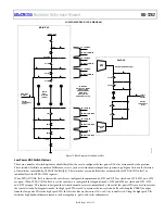
Figure 18 shows the relationship between the R
LOAD
and R
GAIN
settings for the low power TIA. R
LOAD
is configured by setting LPTIACON0,
Bits[12:10]. R
GAIN
is configured by LPTIACON0, Bits[9:5]. When R
LOAD
is large, it uses resistors from the R
GAIN
bank, which reduces the
size of R
GAIN
. See the descriptions in the LPTIACON0 bit fields for details.
Low Power TIA and Potentiostat Amplifiers Current Limit Feature
In addition to the protection diode, the low power TIAs also have a built in current limiting feature. If the current sourced or sunk from
the low power TIAs is greater than the overcurrent limit protection specified in the
data sheet, the amplifiers clamp the
current to this limit. If a sensor on startup attempts to source or sink more than the overcurrent limit, the amplifier clamps the output
current. Do not use this feature more frequently or for longer than specified in the data sheet. See the
specifications.
Low Power TIA Force and Sense Feature
LPTIACONx, Bits[9:5] select different gain resistor values for the low power TIA, labeled as R
TIA
in Figure 16 and Figure 17. The force and
sense connections shown on the feedback path of the low power TIA are used to avoid voltage (I × R) drops on the switches used to
select different R
TIA
settings for the internal R
TIA
.
External R
TIA
Gain Resistor with Low Power TIA Amplifiers
To use an external R
TIA
gain resistor, follow this process:
Connect the external R
TIA
across the RC0_0 and RC0_1 pins for Channel 0. For Channel 1, connect the external R
TIA
across the
RC1_0 and RC1_1 pins.
Clear LPTIACONx, Bits[9:5] = 0b00000 to disconnect the internal R
TIA
from the TIA output terminal.
Close the SW9 switch by setting LPTIASWx, Bit 9 = 1. When using the internal R
TIA
, open the SW9 switch.
LOW POWER DACs
The low power DACs are designed to set the sensor bias voltage. In Figure 15, the sensor bias voltage is the voltage difference between
the reference electrode and sense electrode.
Each low power DAC has two outputs, an output with 12-bit resolution (VBIAS0 pin) and an output with 6-bit resolution (VZERO0 pin). The
low power DACs are made up of two 6-bit string DACs. The main 6-bit string DAC provides the VZERO0 DAC output, and is made up
of 63 resistors. Each resistor is the same value.
The main 6-bit string with the 6-bit subDAC provides the VBIAS0 DAC output. In 12-bit mode, the MSBs select a resistor from the main
string DAC. The top end of this resistor is selected as the top of the 6-bit subDAC, and the bottom end of the selected resistor is
connected to the bottom of the 6-bit subDAC string.
The resistor matching between the 12-bit and 6-bit subDAC means 64 LSB 12-bit (VBIAS0 pin) is equal to one LSB 6-bit (VZERO0 pin).
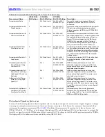
Figure 19 shows the low power DAC structure. The main DAC string shows the 64 resistors that make up the six bits of the VZERO0
output and the six MSBs of the VBIAS output. The main DAC makes up the 6-bit DAC output (VZERO0 output), and is controlled by
LPDACDATx, Bits[17:12]. The output range is 0.2 V to 2.36615 V. The right side of the main DAC block shows the six MSBs of the
12-bit DAC output (VBIAS0 output), which are controlled by LPDACDATx, Bits[11:0]. The voltage steps of these bits are equal to the
6-bit VZERO0 output steps. The 12-bit output is capable of reaching 2.4 V.
The subDAC block shows the 64-resistor string used to generate the six LSBs of the 12-bit output. The low power DACs are controlled
by LPDACCONx, Bits[5:0].


