


Preliminary Technical Data
UG-1828
Rev. PrC | Page 251 of 338
PRINTED CIRCUIT BOARD LAYOUT RECOMMENDATIONS
The ADRV9001 is a highly integrated RF agile transceiver with significant signal conditioning integrated onto one chip. Due to the
integration complexity of the ADRV9001 and its high pin count, careful printed circuit board (PCB) layout is important to optimize
performance. This section provides a checklist of issues to look for and guidelines on how to optimize the PCB to mitigate performance
issues. The goal of this document is to help achieve the best possible performance from the ADRV9001 while reducing board layout
effort. It is assumed that the reader is an experienced analog/RF engineer who understands RF PCB layout and has an understanding of
RF transmission lines as well as low-noise analog design techniques. The ADRV9001 evaluation card is used as the reference for this
information, but all guidelines are best practices that can be applied to other reference designs. This document provides guidelines for
system designers and discusses the following issues relative to layout and power management.
•
PCB material and stack up selection
•
Fan-out and layout guidelines relative to trace widths and spacing
•
Component placement and routing guidelines
•
RF and Data Port transmission line layout
•
Isolation techniques used on the ADRV9001 customer evaluation board
PCB MATERIAL AND STACK UP SELECTION
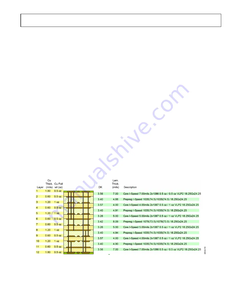
Figure 240 shows the PCB stackup used for the ADRV9001 customer evaluation boards. These boards employ 12 layers to achieve proper
routing and isolation to best demonstrate all device functionality. The dielectric material used is I-SPEED with a thickness of 7 mil on
outer layers. The board design uses the I-SPEED laminate for its low loss tangent at high frequencies. The ground planes under the I-
SPEED laminate (layers 2 and 11) are the reference planes for the transmission lines routed on the outer surfaces. These layers are solid
copper planes under the RF traces with no discontinuities. Layers 2 and 11 are crucial to maintaining the RF signal integrity.
RF traces on the outer layers must be a controlled impedance to get the best performance. These outer layers use 0.5 ounce copper. 0.5
and 1-ounce copper thickness are used for all the inner layers in this board. All ground planes on this board are full copper floods with no
splits except for vias, through-hole components and isolation structures (more on this in later sections).
Layers 3, 5, 7, 9 are mainly used to route power supply domains. The Date Port interface lines are routed on layers 1, 7 and 12. Those
layers have impedance control set to 100Ω differential for the differential LVDS pairs. The remaining digital signals are routed on inner
layers 3, 5, 9 and 10. Table 100 describes details of the trace impedance controls used on different layers.
There are no buried in or blind vias used in this PCB design. All vias used in the PCB design are thru hole type. For vias carrying high
frequency or RF sensitive signals, back drilling technique is applied.
Figure 240. ADRV9001 Customer Evaluation Card Stackup


