ADAV4622
Rev. B | Page 22 of 2
8
I
2
C INTERFACE
The ADAV4622 supports a 2-wire serial (I
2
C compatible)
microprocessor bus driving multiple peripherals. The
ADAV4622 is controlled by an external I
2
C master device,
such as a microcontroller. The ADAV4622 is in slave mode
on the I
2
C bus, except during self-boot. While the ADAV4622
is self-booting, it becomes the master, and the EEPROM, which
contains the ROMs to be booted, is the slave. When the self-
boot process is complete, the ADAV4622 reverts to slave mode
on the I
2
C bus. No other devices should access the I
2
C bus while
the ADAV4622 is self-booting (refer to the Application Layer
section and the Loading a Custom Audio Processing Flow
section).
Initially, all devices on the I
2
C bus are in an idle state, wherein
the devices monitor the SDA and SCL lines for a start condition
and the proper address. The I
2
C master initiates a data transfer
by establishing a start condition, defined by a high-to-low
transition on SDA while SCL remains high. This indicates that
an address/data stream follows. All devices on the bus respond
to the start condition and read the next byte (7-bit address plus
the R/W bit) MSB first. The device that recognizes the transmit-
ted address responds by pulling the data line low during the
ninth clock pulse. This ninth bit is known as an acknowledge
bit. All other devices on the bus revert to an idle condition. The
R/W bit determines the direction of the data. A Logic Level 0
on the LSB of the first byte means the master writes information
to the peripheral. A Logic Level 1 on the LSB of the first byte
means the master reads information from the peripheral. A data
transfer takes place until a stop condition is encountered. A stop
condition occurs when SDA transitions from low to high while
SCL is held high.
The ADAV4622 determines its I
2
C device address by sampling
the SDO0 pin after reset. Internally, the SDO0 pin is sampled by
four MCLKI edges to determine the state of the pin (high or
low). Because the pin has an internal pull-down resistor default,
the address of the ADAV4622 is 0x34 (write) and 0x35 (read).
An alternate address, 0x36 (write) and 0x37 (read), is available
by tying the SDO0 pin to ODVDD via a 10 kΩ resistor. The I
2
C
interface supports a clock frequency up to 400 kHz.
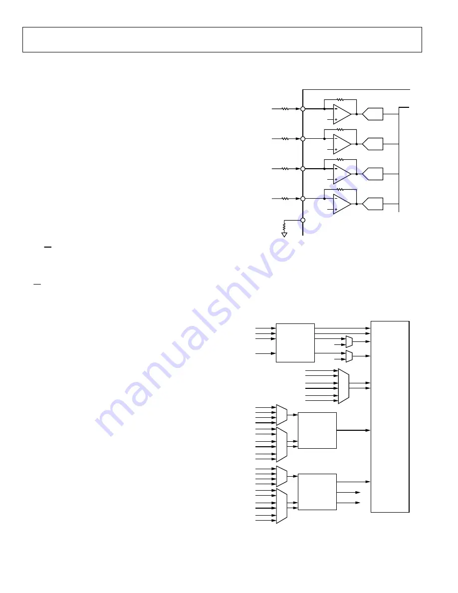
ADC INPUTS
The ADAV4622 has four ADC inputs. By default, these are
configured as two stereo inputs; however, because the audio
processor is programmable, these inputs can be reconfigured.
The ADC inputs are shown in Figure 23. The analog inputs are
current inputs (100 μA rms FS) with a 1.5 V dc bias voltage.
Any input voltage can be accommodated by choosing a suitable
combination of input resistor (R
IN
) and ISET resistor (R
ISET
)
using the formulas
R
IN
=
V
FS rms
/100 μA rms
R
ISET
= 2R
IN
/V
IN
Resistor matching (typically 1%) between R
IN
and R
ISET
is
important to ensure a full-scale signal on the ADC without
clipping.
DC BIAS
1.5V
24-BIT
ADC
AUXIN1L
20k
Ω
ANALOG INPUT
100µA rms
FULL SCALE
DC BIAS
1.5V
24-BIT
ADC
AUXIN1R
20k
Ω
ANALOG INPUT
100µA rms
FULL SCALE
DC BIAS
1.5V
24-BIT
ADC
AUXIN2L
20k
Ω
ANALOG INPUT
100µA rms
FULL SCALE
DC BIAS
1.5V
24-BIT
ADC
AUXIN2R
20k
Ω
ANALOG INPUT
100µA rms
FULL SCALE
R
ISET
20k
Ω
ISET
07
06
8-
0
19
Figure 23. Analog Input Section
I
2
S DIGITAL AUDIO INPUTS
The ADAV4622 has four I
2
S digital audio inputs that are, by
default, synchronous to the master clock. Also available are two
SRCs capable of supporting any nonsynchronous input with a
sample rate between 5 kHz and 50 kHz. Any of the serial digital
inputs can be redirected through the SRC. Figure 24 shows a
block diagram of the input serial port.
SRC2B
SRC2C
LRCLK0
BCLK0
LRCLK1
BCLK1
LRCLK2
BCLK2
SDIN0
SDIN1
SDIN2
SDIN3
LRCLK0
BCLK0
SDIN0
SDIN1
SDIN2
SDIN3
LRCLK1
BCLK1
LRCLK2
BCLK2
SRC1
LRCLK0
BCLK0
SDIN0
SDIN1
SDIN2
SDIN3
LRCLK1
BCLK1
LRCLK2
BCLK2
SRC2
SRC2A
SRC2B
SRC2C
AUDIO
PROCESSOR
0
70
68
-02
1
Figure 24. Digital Input Section


