background image

AD9912 


Rev. D | Page 38 of 40 

OUTLINE DIMENSIONS 

PIN 1
INDICATOR

TOP

VIEW

8.75

BSC SQ

9.00

BSC SQ

1

64

16

17

49

48

32

33

0.50
0.40
0.30

0.50 BSC

0.20 REF

12° MAX

0.80 MAX
0.65 TYP

1.00
0.85
0.80

7.50
REF

0.05 MAX
0.02 NOM

0.60 MAX

0.60 MAX

*4.85

4.70 SQ
4.55

EXPOSED PAD

(BOTTOM VIEW)

*COMPLIANT TO JEDEC STANDARDS MO-220-VMMD-4
 EXCEPT FOR EXPOSED PAD DIMENSION

082908-

B

SEATING

PLANE

PIN 1
INDICATOR

0.30
0.25
0.18

FOR PROPER CONNECTION OF
THE EXPOSED PAD, REFER TO
THE PIN CONFIGURATION AND
FUNCTION DESCRIPTIONS
SECTION OF THIS DATA SHEET.


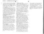
Figure 57. 64-Lead Lead Frame Chip Scale Package [LFCSP_VQ]  

9 mm × 9 mm Body, Very Thin Quad  

(CP-64-1)  

Dimensions shown in millimeters 


COMPLIANT TO JEDEC STANDARDS MO-220-VMMD-4

062209-A

0.25 MIN

1

64

16

17

49

48

32

33

0.50
0.40
0.30

0.50

BSC

0.20 REF

12° MAX

0.80 MAX
0.65 TYP

1.00
0.85
0.80

7.50 REF

0.05 MAX
0.02 NOM

0.60 MAX

0.60

MAX

SEATING

PLANE

PIN 1
INDICATOR

5.36
5.21 SQ
5.06

PIN 1

INDICATOR

0.30
0.23
0.18

FOR PROPER CONNECTION OF
THE EXPOSED PAD, REFER TO
THE PIN CONFIGURATION AND
FUNCTION DESCRIPTIONS
SECTION OF THIS DATA SHEET.

TOP VIEW

EXPOSED

PAD

BOTTOM VIEW

9.10
9.00 SQ
8.90

8.85
8.75 SQ
8.65


Figure 58. 64-Lead Lead Frame Chip Scale Package [LFCSP_VQ]  

9 mm × 9 mm Body, Very Thin Quad  

(CP-64-7)  

Dimensions shown in millimeters 

Summary of Contents for AD9912

Page 1: ...MHz Programmable output divider for CMOS output Serial I O control Excellent dynamic performance Software controlled power down Available in two 64 lead LFCSP packages Residual phase noise 250 MHz 10...

Page 2: ...S Divider Register 0x0100 to Register 0x0106 34 Frequency Tuning Word Register 0x01A0 to Register 0x01AD 34 Doubler and Output Drivers Register 0x0200 to Register 0x0201 36 Calibration User Accessibl...

Page 3: ...pply with system clock PLL HSTL output driver and S divider enabled IAVDD Pin 53 40 48 mA DAC power supply IDVDD Pin 3 Pin 5 Pin 7 205 246 mA Digital core SpurKiller off IDVDD_I O Pin 1 Pin 141 2 3 mA...

Page 4: ...ure 28 and Figure 29 for output swing vs frequency Output Voltage High VOH 2 7 V IOH 1 mA Pin 37 3 3 V Output Voltage Low VOL 0 4 V IOL 1 mA Pin 37 3 3 V Output Voltage High VOH 1 4 V IOH 1 mA Pin 37...

Page 5: ...requency Range 6 100 MHz Multiplication Range 8 132 Integer multiples of 8 Input Duty Cycle 50 Deviating from 50 duty cycle may adversely affect spurious performance Minimum Differential Input Level 6...

Page 6: ...utput 96 dBc 250 kHz 201 1 MHz Output 91 dBc 250 kHz 398 7 MHz Output 86 dBc 250 kHz DIGITAL TIMING SPECIFICATIONS Time Required to Enter Power Down 15 s Time Required to Leave Power Down 18 s Reset A...

Page 7: ...s is a stress rating only functional operation of the device at these or any other conditions above those indicated in the operational section of this specification is not implied Exposure to absolute...

Page 8: ...configured under program control and do not have internal pull up pull down resistors 11 19 23 to 26 29 30 36 42 44 45 53 I Power AVDD Analog Supply Connect to a nominal 1 8 V supply 12 13 15 16 17 18...

Page 9: ...nal should be filtered and sent back on chip through the FDBK_IN input This pin has an internal 50 pull down resistor 51 O Differential output DAC_OUTB Complementary DAC Output This signal should be f...

Page 10: ...0 80 90 100 SIGNAL POWER dBm 20 1MHz 79dBc 500MHz 3kHz 10kHz CARRIER SFDR FREQ SPAN RESOLUTION BW VIDEO BW Figure 5 Wideband SFDR at 20 1 MHz SYSCLK 1 GHz SYSCLK PLL Bypassed 06763 006 0 100 200 300 4...

Page 11: ...igure 11 Narrow Band SFDR at 398 7 MHz SYSCLK 1 GHz Wenzel Oscillator SYSCLK PLL Bypassed 06763 012 100 1k 10k 100k 1M 10M 100M FREQUENCY OFFSET Hz 80 90 100 110 120 130 140 150 160 PHASE NOISE dBc Hz...

Page 12: ...790fs Figure 17 Absolute Phase Noise Using CMOS Driver at 1 8 V SYSCLK 1 GHz Wenzel Oscillator SYSCLK PLL Bypassed 06763 018 250 375 500 625 750 875 1000 SYSTEM CLOCK FREQUENCY MHz 800 700 600 500 40...

Page 13: ...olute Phase Noise of Unfiltered DAC Output fOUT 171 MHz SYSCLK Driven by a 1 GHz Wenzel Oscillator SYSCLK PLL Bypassed 06763 054 100 1k 10k 100k 1M 10M 100M FREQUENCY OFFSET Hz 125 115 135 145 155 165...

Page 14: ...gure 29 CMOS Output Driver Peak to Peak Amplitude vs Toggle Rate AVDD3 3 3 V with 20 pF Load 06763 024 0 0 5 1 0 1 5 2 0 2 5 TIME ns 0 4 0 6 0 2 0 0 2 0 4 0 6 AMPLITUDE V FREQUENCY 600MHz tRISE 20 80...

Page 15: ...AD9912 SELF BIASING SYSCLK INPUT CRYSTAL MODE 10pF 06763 029 10pF REFER TO CRYSTAL DATA SHEET Figure 35 SYSCLK Input Xtal AD9912 SELF BIASING SYSCLK INPUT 0 1 F 0 1 F 100 06763 030 CLOCK SOURCE WITH...

Page 16: ...ut frequency at 50 of fS where fS is the DAC sample rate but a practical limitation of 40 of fS is generally recommended to allow for the selectivity of the required off chip reconstruction filter The...

Page 17: ...ram in Figure 41 The peak output current derives from a combination of two factors The first is a reference current IDAC_REF that is established at the DAC_RSET pin and the second is a scale factor th...

Page 18: ...red output frequency plus 20 rolls off as steeply as possible and then maintains significant though not complete rejection of the remaining images Depending on how close unwanted spurs are to the desi...

Page 19: ...input pins becomes the internal DAC sampling clock fS after passing through an internal buffer It is important to note that when bypassing the system clock PLL the LOOP_FILTER pin Pin 31 should be pul...

Page 20: ...ng the range to 33 Care should be taken when choosing these values so as not to exceed the maximum input frequency of the SYSCLK PLL phase detector or SYSCLK PLL doubler These values can be found in t...

Page 21: ...for frequencies up to 150 MHz The signal path for the CMOS clock driver can either include or bypass the CMOS output divider If the CMOS output divider is bypassed the HSTL and CMOS drivers are the s...

Page 22: ...to Bit 3 of Register 0x0500 Register 0x0505 2 Turn off the fundamental by setting Bit 7 of Register 0x0013 and enable the SpurKiller channel by setting Bit 7 of Register 0x0500 Register 0x0505 3 Adjus...

Page 23: ...51 2 still air 0 1 C W The AD9912 is specified for a case temperature TCASE To ensure that TCASE is not exceeded an airflow source can be used Use the following equation to determine the junction temp...

Page 24: ...es that are used both to address an internal 8 16 ROM and to select the SYSCLK mode see Table 8 The ROM contains eight 16 bit DDS frequency tuning words FTWs one of which is selected by the state of t...

Page 25: ...e about 25 mA At a minimum a ferrite bead should be used to isolate these from other 3 3 V supplies with a separate regulator being ideal 1 8 V SUPPLIES DVDD Pin 3 Pin 5 and Pin 7 These pins should be...

Page 26: ...he serial control port state machine enters a wait state until all data has been sent If the system controller decides to abort the transfer before all of the data is sent the state machine must be re...

Page 27: ...r map that is written to or read from during the data transfer portion of the communications cycle The AD9912 uses all of the 13 bit address space For multibyte transfers this address is the starting...

Page 28: ...CARE DON T CARE DON T CARE DON T CARE D7 D6 D5 D4 D3 D2 D1 D0 D7 D6 D5 D4 D3 D2 D1 D0 D7 D6 D5 D4 D3 D2 D1 D0 D7 D6 D5 D4 D3 D2 D1 D0 06763 057 Figure 52 Serial Control Port Read MSB First 16 Bit Inst...

Page 29: ...rameter Description tCLK Period of SCLK tDV Read data valid time time from falling edge of SCLK to valid data on SDIO SDO tDS Setup time between data and rising edge of SCLK tDH Hold time between data...

Page 30: ...Reserved 0x00 0x0012 M AC Reset DDS reset 0x00 0x0013 M PD fund DDS S div 2 reset S divider reset 0x00 System clock 0x0020 N divider N divider Bits 4 0 0x12 0x0021 Reserved 0x00 0x0022 PLL parameters...

Page 31: ...x00 Harmonic spur reduction 0x0500 M Spur A HSR A enable Amplitude gain 2 Spur A harmonic Bits 3 0 0x00 0x0501 M Spur A magnitude Bits 7 0 0x00 0x0503 M Spur A phase Bits 7 0 0x00 0x0504 M Spur A phas...

Page 32: ...ive registers instead of the buffer 1 reads the buffered values that take effect during the next I O update 0 reads values that are currently in effect Register 0x0005 Serial Options Self Clearing Tab...

Page 33: ...scription 4 0 N divider These bits set the feedback divider for system clock PLL There is a fixed divide by 2 preceding this block as well as an offset of 2 added to this value Therefore setting this...

Page 34: ...setting is greater than 65 536 or if the signal on FDBK_IN is greater than 400 MHz this bit must be set FREQUENCY TUNING WORD REGISTER 0x01A0 TO REGISTER 0x01AD Register 0x01A0 to Register 0x01A5 Rese...

Page 35: ...y Register 0x01AB FTW0 Frequency Tuning Word Continued Table 29 Bits Bit Name Description 47 40 FTW0 These registers contain the FTW frequency tuning word for the DDS The FTW determines the ratio of t...

Page 36: ...ed Register 0x040B DAC Full Scale Current Table 34 Bits Bit Name Description 7 0 DAC full scale current DAC full scale current Bits 7 0 See the Digital to Analog DAC Output section Register 0x040C DAC...

Page 37: ...ting this bit doubles the gain of the cancelling circuit and also doubles the minimum step size 5 4 Reserved Reserved 3 0 Spur B harmonic Spur B Harmonic 1 to Spur B Harmonic 15 Allows user to choose...

Page 38: ...T Figure 57 64 Lead Lead Frame Chip Scale Package LFCSP_VQ 9 mm 9 mm Body Very Thin Quad CP 64 1 Dimensions shown in millimeters COMPLIANT TO JEDEC STANDARDS MO 220 VMMD 4 062209 A 0 25 MIN 1 64 16 17...

Page 39: ...CPZ REEL71 2 40 C to 85 C 64 Lead Lead Frame Chip Scale Package LFCSP_VQ CP 64 7 AD9912BCPZ1 40 C to 85 C 64 Lead Lead Frame Chip Scale Package LFCSP_VQ CP 64 1 AD9912BCPZ REEL71 40 C to 85 C 64 Lead...

Page 40: ...AD9912 Rev D Page 40 of 40 NOTES 2007 2009 Analog Devices Inc All rights reserved Trademarks and registered trademarks are the property of their respective owners D06763 0 11 09 D...

Reviews: