background image

Evaluation Board User Guide 

UG-075


Rev. 0 | Page 9 of 16 

REGISTER W/R BOX 

The 

REGISTER W/R

 (write/read) box has four buttons and 

three check boxes. 

The 

WRITE

 button transfers the values stored in the evaluation 

software to the evaluation board. It blinks red when register 
values have changed. 

The 

READ

 button transfers the values stored in the evaluation 

board to the evaluation software.  

The 

UPDATE

 button issues an I/O update command by writing 

0x01 to Register 0x232.  

Selecting the 

All

 check box transfers all of the registers when 

the 

WRITE

 button is clicked. When this check box is cleared, 

only the registers whose value has changed are written. 

Selecting the 

Auto

 check box adjacent to the 

WRITE

 box  

forces the evaluation software to write the register changes  
to the evaluation board automatically when they occur. 

Selecting the 

Auto

 check box adjacent to the 

UPDATE

 box 

forces the evaluation software to issue an I/O update command 
whenever registers are written to the AD951x. It is checked by 
default.  

SYNC, PD (POWER DOWN), AND RESET BUTTONS 

The 

SYNC

PD

, and 

RESET

 buttons allow you to control the 

SYNC, PD, and RESET pins on the AD951x. 

Each button has three options: 

Strobe

Latch

, and 

Release

Strobe

 activates the pin, and then releases it. 

Latch

 holds  

the pin active until the 

Release

 command is issued. 

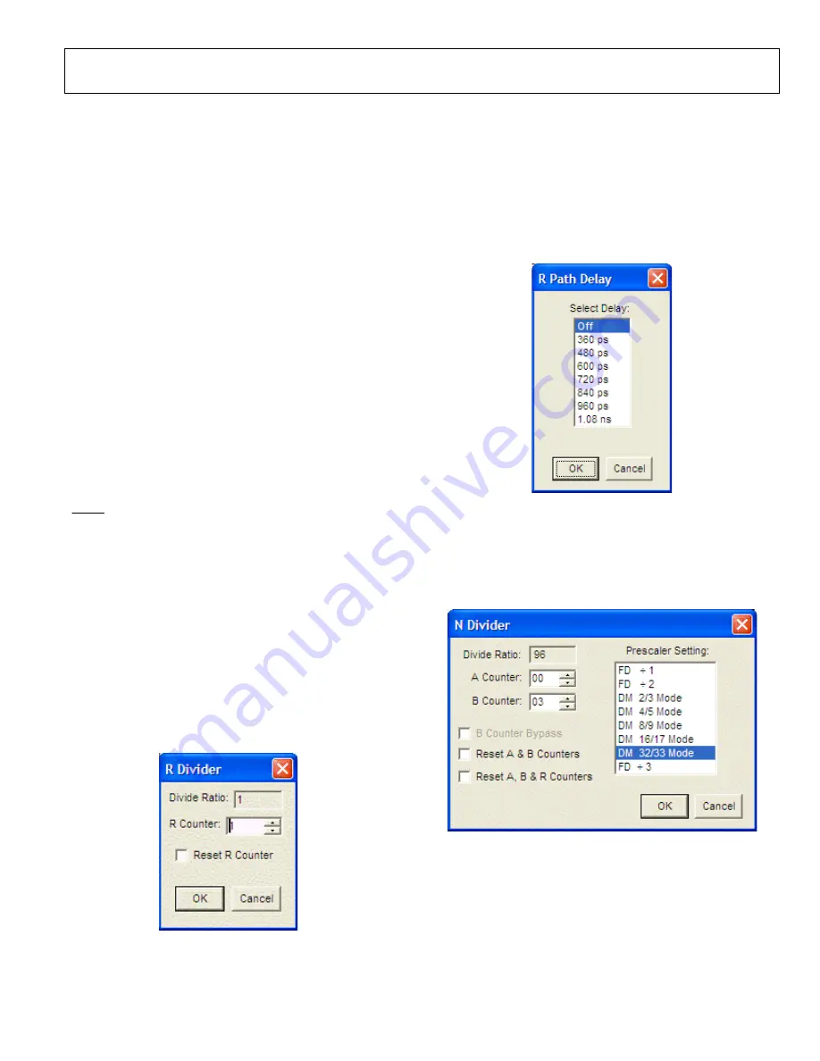
REFERENCE (R) DIVIDER WINDOW 

The 

R Divider

 window shown in Figure 12 is accessed by 

clicking the 

R DIVIDER

 box on the main window. It allows  

you to set the reference divider. If this box is colored gray, the 
PLL is off. To turn the PLL on, click the 

PLL MODE

 box at  

the top of the main window, and select 

Norm Op

.  

The 

R Divider

 window has a check box for holding the 

R divider in reset. When the R divider is held in reset, the  
PLL loop is opened. Therefore, this feature is seldom used.  

087

45-

009


Figure 12. R Divider Window 

R AND N DELAY WINDOW 

The AD951x features two delay circuits (one on the reference 
divider path, and one on the feedback divider path) that allow 
the user to control the static phase offset between the reference 
input and the PLL output. The 

R Path Delay

 window shown in 

Figure 13 is accessed by clicking the 

R DELAY

 button on the 

main screen. The 

R DELAY

 box is identical to the 

N DELAY


box. These delay settings allow you to vary the static phase 
offset of the PLL. 

08

74

5-

010


Figure 13. R Path Delay Window 

FEEDBACK (N) DIVIDER WINDOW 

The reference divider window shown in Figure 14 is accessed by 
clicking the 

N DIVIDER

 box on the main screen. If this box is 

colored gray, the PLL is off. To turn the PLL on, click the 

PLL 

MODE

 box at the top of the main screen, and select 

Norm Op

087

45

-011


Figure 14. N Divider Window 

The various modes of the N divider are described in detail in 
the AD951x data sheet. For most applications, the 8/9 or 16/17 
dual modulus modes are used. For applications requiring a 
divider value larger than 131,119, the 32/33 mode is provided. 
Different applications require different settings, and you can 
experiment with the different settings. 

www.BDTIC.com/ADI

Summary of Contents for AD9516

Page 1: ...16 x AD9517 x and AD9518 x are very low noise PLL clock synthesizers featuring an integrated VCO clock dividers and up to 14 outputs The AD9516 features automatic holdover and a flexible reference inp...

Page 2: ...tware Components 7 Main Window 7 PLL Reference Input Window 8 PLL Configuration Window 8 REFMON STATUS and LD Buttons 8 Register W R Box 9 SYNC PD Power Down and RESET Buttons 9 Reference R Divider Wi...

Page 3: ...damaged SIGNAL CONNECTIONS To connect signals use the following steps 1 Connect a signal generator to the J10 SMA connector By default the reference inputs on this evaluation board are ac coupled and...

Page 4: ...ware Depending on whether the evaluation board was found by the software either light blue text appears in a pop up window indicating that the evaluation board was found or red text appears indicating...

Page 5: ...ox found at the top of the main window see Figure 8 2 Enter the intended reference input frequency in megahertz in the REF 1 MHz box at the upper left corner of the main window 3 Click the triangular...

Page 6: ...is setting normally does not need to be modified 10 Set the VCO divider by clicking the green VCO box in the center of the main window immediately to the left of the Cal VCO button 11 Power down unuse...

Page 7: ...listed in the following sections and each of these has its own window From the main window each functional block can be accessed by clicking that block in the main window When a subwindow closes after...

Page 8: ...The SyncB Counter Reset Mode section indicates whether the R A and B counters are reset when the SYNC pin is activated and controls R0x019 7 6 See the AD951x data sheet for more details The ReadBack...

Page 9: ...e R DIVIDER box on the main window It allows you to set the reference divider If this box is colored gray the PLL is off To turn the PLL on click the PLL MODE box at the top of the main window and sel...

Page 10: ...tter with the 1 3 ns antibacklash pulse width setting Setting the lock detect counter to values greater then 5 PFD cycles can be useful in applications where the loop bandwidth is low and the lock det...

Page 11: ...g However to have the new phase take effect the SYNC signal needs to be toggled by using the SYNC button in the lower left corner of the main window 08745 015 Figure 18 Divider 1 Settings Window LVPEC...

Page 12: ...f delay is shown in the right half of the window The feature is described in detail in the AD951x data sheet 08745 017 08745 018 Figure 22 Output 6 Delay Window DEBUG WINDOW The Debug window shown in...

Page 13: ...w allows you to select which evaluation board the software is controlling Click Refresh List to detect a recently connected evaluation board see Figure 25 08745 020 Figure 25 Select USB Device Window...

Page 14: ...Ethernet line cards as well as applications where the reference clock is relatively high jitter the low loop BW loop filter shown in Table 3 is a better choice It has a flat transfer function with pe...

Page 15: ...reference clock is noisy or for cases where the frequency planning requires a phase detector frequency of 1 MHz or lower Table 3 AD9516 Evaluation Board Low Loop Bandwidth Clock Cleanup Filter Compon...

Page 16: ...of evaluation boards Information furnished by Analog Devices is believed to be accurate and reliable However no responsibility is assumed by Analog Devices for its use nor for any infringements of pa...

Reviews: