background image

AMI Baby Voyager User's Guide

79

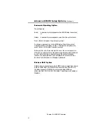
Hard Disk Format,

 Continued

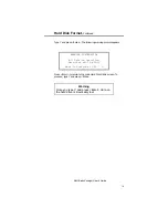
Type 

Y

 and press <Enter>. The following warning prompt appears.

WARNING INFORMATION

All Data on Specified

Hard disk will be LOST

Want to Continue (Y/N) ? N

Press <Enter> to return to the main Hard Disk Utility screen. To

proceed, type 

Y

 and press <Enter>.

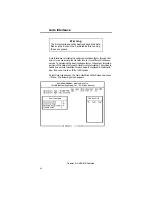
Warning

Once you type 

Y

 and press <Enter>, data on

the hard drive is irrevocably lost.

Summary of Contents for 39 Series

Page 1: ...AMI Series 39 Series 39 Baby Voyager Baby Voyager 80486 Motherboard 80486 Motherboard User s Guide User s Guide MAN 639 5 26 92 ...

Page 2: ... AMI shall not be liable in tort or contract for any loss or damage direct incidental or consequential Please see the AMI Warranty Registration Card shipped with this product for full warranty details L i m i t a t i o n s o f L i a b i l i t y L i m i t a t i o n s o f L i a b i l i t y In no event shall AMI be held liable for any loss expenses or damages of any kind whatsoever whether direct ind...

Page 3: ...9 Step 6 Connect the Keyboard 20 Step 7 Connect Cables 21 Connect the Reset Button Connector 21 Connect the Speaker Cable 22 Connect the Keyboard Lock Connector 22 J23 Turbo LED 22 Serial Port Connectors 24 Step 8 Install Floppy Drive 26 Step 9 Install Hard Disk 28 Step 10 Install Adapter Cards 29 Adapter Card Pinout 29 Step 11 Perform Initial Test and Configuration 31 In Case of Errors 32 Chapter...

Page 4: ...onfiguration 53 Hard Disk Parameter Table 54 Floppy 56 Monitor 56 Keyboard 56 Section 3 Advanced CMOS Setup 57 Memory Test Tick Sound 60 Hard Disk Type 47 RAM Area 61 System Boot Up Num Lock 62 Weitek Processor 62 Floppy Drive Seek At Boot 62 System Boot Up Sequence 62 System Boot Up CPU Speed 63 Fast Gate A20 Option 63 Password Checking Option 64 Shadow RAM Option 64 Section 4 Advanced Chip Set S...

Page 5: ...s manual is not meant to be read by the computer owner who purchases a computer with the Baby Voyager motherboard It is assumed that you the computer manufacturer will use this manual as a sourcebook of information and that parts of this manual will be included in the computer owner s manual T e c h n i c a l S u p p o r t T e c h n i c a l S u p p o r t If a Baby Voyager motherboard fails to oper...

Page 6: ...Preface vi ...

Page 7: ... approximately 8 55 by 13 inches It is similar in size to a standard XT or baby AT motherboard The mounting hole locations allow this motherboard to be used with baby AT or XT chassis The height of the board components is no more than 1 inches Allow 2 inches of clearance for the power supply connectors See the following graphic ...

Page 8: ...peeds can be changed via the keyboard by the keystroke combinations Ctrl Alt and Ctrl Alt These keystrokes can be changed by the OEM via AMIBCP AMI BIOS Configuration Program C a c h e M e m o r y C a c h e M e m o r y The external cache memory size can be either 64 KB or 256 KB Up to 32 MB of system memory can be cached There are 0 wait states for cache memory read and write Burst mode is support...

Page 9: ...ller two serial ports and one parallel port on the motherboard S y s t e m B I O S S y s t e m B I O S The AMI Baby Voyager uses an AMI Hi Flex BIOS with built in Setup configuration utility and hard disk drive utilities Through the AMI BIOS Setup an end user can configure up to two user definable hard disk drive types The end user can easily configure systems with no video monitor keyboard or flo...

Page 10: ...c t i o n s The AMI Baby Voyager supports all standard ISA functions such as those listed below plus nonstandard functions seven Direct Memory Access DMA channels Channels 0 3 are used for 8 bit data transfer and Channels 5 7 are used for 16 bit data transfers sixteen interrupt levels eleven levels of interrupt are supported including IRQ3 IRQ7 IRQ9 IRQ12 IRQ14 and IRQ15 three programmable timers ...

Page 11: ... system memory system memory refresh from channel microprocessors R e a l T i m e C l o c k R e a l T i m e C l o c k The AMI Baby Voyager has a standard AT type real time clock that is crystal controlled K e y b o a r d K e y b o a r d The AMI Baby Voyager has a standard 5 pin DIN connector for an AT compatible keyboard The Baby Voyager also has a keyboard lock function to prevent unauthorized ac...

Page 12: ...Chapter 1 Introduction 6 ...

Page 13: ...or instead of the anti static mat Similarly a strip of conductive aluminum foil wrapped around the wrist and grounded through a 1 megohm resistor serves the same purpose 3 Inside the carton the Baby Voyager motherboard is packed in an anti static bag and sandwiched between sheets of sponge Remove the sponge and remove the anti static bag Place the Baby Voyager motherboard on a grounded anti static...

Page 14: ...Chapter 2 Installation 8 Baby Voyager Layout ...

Page 15: ...ons Page 10 2 Install memory Page 13 3 Install coprocessors Page 16 4 Install motherboard Page 17 5 Connect the power supply Page 19 6 Connect the keyboard Page 21 7 Connect cables Page 22 8 Install floppy drive Page 27 9 Install hard disk drive Page 29 10 Install adapter cards Page 30 11 Perform initial test and configuration Page 32 Standoffs and mounting screws are not supplied with the AMI 804...

Page 16: ...s no effect if an EGA or VGA adapter is used 3 Video Shadow The video ROM segment beginning at C000h is copied from the BIOS ROM to faster RAM for faster video operation This switch is factory set to ON 4 ROM BIOS Shadow Similar to video shadow except the entire system BIOS 64 KB in length is shadowed This switch is factory set to ON 5 6 7 8 Memory configuration Positions 5 6 7 and 8 are used with...

Page 17: ...for the parallel port this is the default value J 3 5 E n a b l e B u r s t M o d e J 3 5 E n a b l e B u r s t M o d e J35 is factory hardwired to enable burst mode J 1 9 B u r s t A d d r e s s 2 J 1 9 B u r s t A d d r e s s 2 J19 is factory hardwired to pins 2 and 3 J 2 0 B u r s t A d d r e s s 3 J 2 0 B u r s t A d d r e s s 3 J20 is factory hardwired to pins 2 and 3 J 2 8 B u s C l o c k S ...

Page 18: ...ROMs J 3 6 6 4 K 2 5 6 K C a c h e S e l e c t J 3 6 6 4 K 2 5 6 K C a c h e S e l e c t J36 is a 2 pin single inline berg Make sure J36 is open to select 64 KB of cache memory Short pins 1 2 for 256 KB of cache memory J 2 1 a n d J 2 2 C a c h e A d d r e s s S e l e c t J 2 1 a n d J 2 2 C a c h e A d d r e s s S e l e c t J21 and J22 are 3 pin single inline bergs Short pins 1 2 if 256 KB of cac...

Page 19: ...4 MB 8 MB 16 MB and 32 MB memory configurations on the motherboard using SIMMs The following table describes switch settings for the Baby Voyager memory configurations Bank 0 Bank 1 Switch 5 Switch 6 Switch 7 Switch 8 J4 J5 RAM 256 KB ON ON ON ON 2 3 2 3 1 MB 256 KB 256 KB ON OFF ON ON 2 3 2 3 2 MB 1 MB ON ON ON OFF 2 3 1 2 4 MB 1 MB 1 MB ON OFF ON OFF 2 3 1 2 8 MB 4 MB ON ON OFF OFF 1 2 1 2 16 MB...

Page 20: ...u m b e r s S I M M P a r t N u m b e r s Memory Type Manufacturer Part Number 256 K x 9 Siemens HYB514256AJ 70 1 MB x 9 Fujitsu MB 85235 70 Toshiba THM91000AS 70 NEC MC 42100A9 70 Siemens HYM910005 70 4 MB x 9 Toshiba THM94000S 70 80 NEC MC 85235 70 80 OKI MSC2340 74059 70 80 ...

Page 21: ... These sockets can be filled with 256 KB x 9 1 MB x 9 or 4 MB x 9 SIMMs Use only one type of module to fill each bank Place the AMI 80486 Baby Voyager motherboard on an anti static mat With the component side of the SIMM facing you firmly push the card into the socket When properly inserted the SIMM clicks into place as the latching pins engage See the following figure ...

Page 22: ...t h e W T K 4 1 6 7 o n t h e M o t h e r b o a r d U14 is the empty 121 pin PGA socket labeled WEITEK between the cache memory and microprocessor Pin 1 of the socket is on a chamfered corner that corresponds to pin 1 of the Weitek which also is on a chamfered corner Check for bent pins on the coprocessor Gently straighten any bent pins using a pair of pliers Install the component into the socket ...

Page 23: ...le pattern on the IBM XT motherboard Place the chassis for the Baby Voyager motherboard on an anti static mat Connect the chassis to ground to avoid static damage during installation Connect an alligator clip with a wire lead to any unpainted part of the chassis Ground the other end of the lead at the same point as the mat and the wristband Rotate the chassis so that the front is to the right and ...

Page 24: ...he slots provided for them If the standoffs are properly locked the motherboard should not slide It should also rest level with the chassis The far edge should fit the slots in the plastic clips Place the two mounting screws in the holes provided for them and tighten them If necessary shift the motherboard slightly to align the mounting holes on the motherboard with the holes on the chassis See th...

Page 25: ...ould have built in filters to suppress radiated emissions The filters can help the system pass the appropriate FCC certification testing The power supply is connected to P1 and P2 on the motherboard The connectors should be keyed to prevent connecting the plugs to the wrong connectors The keys on the connector must be cut to fit on some power supplies See the following figure for the location of c...

Page 26: ...Chapter 2 Installation 20 ...

Page 27: ...5 pin DIN socket see the graphic below and is labeled KEYBRD and J3 on the motherboard It accepts a regular IBM AT compatible keyboard A 5 pin DIN to 6 pin mini DIN converter is needed to connect a PS 2 type keyboard Pin Assignments 1 Keyboard clock 2 Keyboard data 3 Not used 4 Ground 5 VCC ...

Page 28: ...s is labeled to identify the pin orientation when plugging in cables See the following graphic L o c a t i n g P i n 1 L o c a t i n g P i n 1 The following cables should be connected to the motherboard from the chassis Reset Switch cable to J12 Speaker cable to J13 Keyboard Lock cable to J15 Turbo LED cable to J23 External Battery Connector to J2 C o n n e c t t h e R e s e t B u t t o n C o n n ...

Page 29: ...t t h e K e y b o a r d L o c k C o n n e c t o r C o n n e c t t h e K e y b o a r d L o c k C o n n e c t o r J15 is a 5 pin single inline berg The keyboard lock allows the user to lock the keyboard protecting the system from unauthorized use This connector is keyed with a blank hole Pin 1 on the motherboard is labeled with a plus sign Pin Description 1 LED power 2 Key 3 Ground 4 Keyboard Lock 5...

Page 30: ...ial or parallel port controller is found the onboard serial or parallel port respectively is disabled Be sure to properly connect the cables to the berg connectors Pin one of each of the bergs is marked with a 1 Pin one of the cable is usually denoted by a colored stripe on the cable J 1 I D E A c t i v i t y I n d i c a t o r L E D J 1 I D E A c t i v i t y I n d i c a t o r L E D J1 is a 2 pin s...

Page 31: ...These connectors provide an AT compatible serial port interface The connecting cable is a 10 pin double row ribbon that connects the motherboard to a male 9 pin D sub connector fastened to the chassis The serial port pinout is shown below Pin Use Pin Use 1 Carrier Detect 6 Data Set Ready 2 Receive Data 7 Request to Send 3 Transmit Data 8 Clear to Send 4 Data Terminal Ready 9 Ring Indicator 5 GND 1...

Page 32: ...BE 14 AUTOFEED 2 PD0 15 ERROR 3 PD1 16 INIT 4 PD2 17 SLCTIN 5 PD3 18 GND 6 PD4 19 GND 7 PD5 20 GND 8 PD6 21 GND 9 PD7 22 GND 10 ACK 23 GND 11 BUSY 24 GND 12 PE 25 GND 13 SLCT 26 N C J 2 E x t e r n a l B a t t e r y C o n n e c t o r J 2 E x t e r n a l B a t t e r y C o n n e c t o r The AMI Baby Voyager does not have room for a battery on the motherboard J2 is a 4 pin berg that connects to a 6 v...

Page 33: ...stalled The following graphic shows the P6 floppy connector and 34 pin cable Pin 1 of Connector Cable The AMI Baby Voyager supports 3 and 5 floppy disk drive in low density 360 KB 720 KB and high density 1 2 MB 1 44 MB Up to two floppy disk drives can be connected to the interface The connecting cable is a 34 pin ribbon connector with two 34 pin edge connectors for connection to the floppy disk dr...

Page 34: ...12 FDSEL1 13 GND 14 FDSEL0 15 GND 16 MOTOR1 17 GND 18 DIR 19 GND 20 STEP 21 GND 22 WDATA 23 GND 24 WGATE 25 GND 26 TRK0 27 GND 28 WRPROT 29 GND 30 RDATA 31 GND 32 HDSEL 33 GND 34 DSKCHNG T w i s t i n F l o p p y C a T w i s t i n F l o p p y C a b l e b l e Floppy B to Floppy A Floppy B to Floppy A Floppy B to Floppy A Floppy B to Floppy A 10 to 16 12 to 14 14 to 12 16 to 10 11 to 15 13 to 13 15 ...

Page 35: ...he onboard IDE interface to use an ISA bus ESDI RLL or MFM hard disk controller The P7 pinout is Pin Use Pin Use 1 RESET 2 GND 3 DATA7 4 DATA8 5 DATA6 6 DATA9 7 DATA5 8 DATA10 9 DATA4 10 DATA11 11 DATA3 12 DATA12 13 DATA2 14 DATA13 15 DATA1 16 DATA14 17 DATA0 18 DATA15 19 GND 20 KEY N C 21 N C 22 GND 23 IOW 24 GND 25 IOR 26 GND 27 N C 28 ALE 29 N C 30 GND 31 INT14 32 IOCS16 33 HA1 34 N C 35 HA0 36...

Page 36: ...patible 8 bit or 16 bit adapter card These cards plug into the expansion slots on the motherboard A d a p t e r C a r d A d a p t e r C a r d P i n o u t P i n o u t Pin Use Pin Use A1 IOCHCK B1 GND A2 SD07 B2 RSTDRV A3 SD06 B3 5 A4 SD05 B4 IRQ9 A5 SD04 B5 5 A6 SD03 B6 DREQ2 A7 SD02 B7 12 A8 SD01 B8 OWS A9 SD00 B9 12 A10 IOCHRDY B10 GND A11 AEN B11 SMEMW A12 SA19 B12 SMEMR A13 SA18 B13 IOW A14 SA1...

Page 37: ...ont d Pin Use Pin Use C1 SBHE D1 MEMCS16 C2 LA23 D2 IOCS16 C3 LA22 D3 IRQ10 C4 LA21 D4 IRQ11 C5 LA20 D5 IRQ12 C6 LA19 D6 IRQ13 C7 LA18 D7 IRQ14 C8 LA17 D8 DACK0 C9 MEMR D9 DREQ0 C10 MEMW D10 DACK5 C11 SD08 D11 DREQ5 C12 SD09 D12 DACK6 C13 SD10 D13 DREQ6 C14 SD11 D14 DACK7 C15 SD12 D15 DREQ7 C16 SD13 D16 5 C17 SD14 D17 MASTER C18 SD15 D18 GND ...

Page 38: ...a r t t h e T e s t Plug everything in and turn on the switch If there are any signs of a problem turn off the unit immediately Reinstall the connectors The fuse may have to be reset Call AMI Technical Support if there are additional problems B I O S E r r o r s B I O S E r r o r s If the system operates normally a display should appear on the monitor The BIOS Power On Self Test POST should run If...

Page 39: ... configuration or hardware The beeps are part of a Beep Code see page 35 that almost always indicates a bad component or that the system must be reconfigured If a beep code sounds make sure the affected part is properly seated and connected Error messages can also appear on the monitor Displayed messages are described on page 36 Recheck the system configuration or the connections to assure that th...

Page 40: ...herboard for normal operations and System Configuration Verification compare defined configuration with hardware actually installed B I O S E r r o r R e p o r t i n g B I O S E r r o r R e p o r t i n g The AMI Hi Flex BIOS performs the various diagnostic checks at the time the system is powered up Errors are reported If Then the error occurs before the display device is initialized a series of b...

Page 41: ...KB block of memory 3 beeps Base 64 KB Memory Failure Memory failure in first 64 KB 4 beeps Timer Not Operational A memory failure occurred within the first 64 KB of memory or Timer 1 on the motherboard is not functioning 5 beeps Processor error The CPU Central Processing Unit on the motherboard has generated an error 6 beeps 8042 Gate A20 Failure Gate A20 on the keyboard controller 8042 contains t...

Page 42: ...e address decoding circuitry on the motherboard C Drive Error No response from hard disk drive C Drive C may be missing If installed run the Hard Disk Utility to correct this problem Also check the C hard disk type in Standard CMOS Setup to make sure that the hard disk drive type is correct C Drive Failure No response from hard disk drive C Replace drive C Cache Memory Bad Do Not Enable Cache Cach...

Page 43: ...l on the motherboard DMA 2 Error An error has occurred with the second DMA channel on the motherboard FDD Controller Failure The BIOS is not able to communicate with the floppy disk drive controller Check all appropriate connections after the system is powered down HDD Controller Failure The BIOS cannot communicate with the hard disk drive controller Check all connectors after the system is powere...

Page 44: ...n Board Parity Error There is a parity error in motherboard memory The message format is ON BOARD PARITY ERROR ADDR HEX XXXX where XXXX is the hex address where the error occurred Onboard means that it is part of motherboard memory Run AMI Diag to find and correct memory problems Parity Error There is a parity error in system memory but the address of the error cannot be determined Run memory diag...

Page 45: ...I O D e v i c e s M a n u a l l y C o n f i g u r i n g I O D e v i c e s The BIOS is not able to detect some MFM or ESDI hard disk drive controllers that have their own onboard BIOS This can cause I O address port conflicts To avoid I O port conflicts the end user can disable any of the onboard I O devices via the BIOS Advanced Chip Set Setup U s i n g a n A d a p t e r C a r d t h a t h a s T w ...

Page 46: ...ining two addresses to the onboard serial ports with SER1 assigned to the higher of COM port If such an adapter card is installed in a Baby Voyager remove the jumpers from J6 and J9 to disable IRQ3 and IRQ4 U s i n g T w o U s i n g T w o O f f B o a r d S e r i a l P o r t s a n d T w o O f f B o a r d S e r i a l P o r t s a n d T w o O n b o a r d P o r t s O n b o a r d P o r t s Since only tw...

Page 47: ...rd serial ports to IRQ4 and both onboard serial ports to IRQ3 If COM1 3F8h and COM2 2F8h are selected as the offboard COM ports SER1 on the motherboard is assigned to COM3 3E8h and SER2 on the motherboard is assigned COM4 2E8 U s i n g T w o U s i n g T w o O f f b o a r d S e r i a l P o r t s O f f b o a r d S e r i a l P o r t s To use only the two offboard serial ports change the I O port assi...

Page 48: ...s driven the bus signal for more than 7 8 microseconds BIOS Configuration Summary Screen The AMI Hi Flex BIOS displays a screen that should look like the following when the POST routines are successfully completed System Configuration C Copyright 1985 1991 American Megatrends Inc Main Processor Numeric Coprocessor Floppy Drive A Floppy Drive B Display Type ROM BIOS Date 80486 Present 1 2 MB 1 44 M...

Page 49: ... X X X X X X X X X X X X X X X X X X X X X A BIOS Identification String is displayed at the left bottom corner of the screen Press Ins during system boot to display two additional BIOS Identification Strings These strings contain the options installed in the AMI BIOS If a problem occurs copy these numbers on a sheet of paper before consulting the AMI Technical Support Department at 404 263 8181 Wh...

Page 50: ...e the OEM can modify these keystroke combinations via AMIBCP The above values are merely the default settings E n a b l e C a c h e M e m o r y E n a b l e C a c h e M e m o r y Both external and internal cache memory can be enabled by pressing Ctrl Alt Shift or disabled by pressing Ctrl Alt Shift The OEM can modify these keystroke combinations via AMIBCP The above values are merely the default se...

Page 51: ...a n c e d C h i p S e t S e t u p A d v a n c e d C h i p S e t S e t u p Advanced Chip Set Setup configures chip set specific features and is discussed on page 67 Advanced CMOS and Advanced Chip Set Setup Features D e f a u l t S e t t i n g s D e f a u l t S e t t i n g s Every option in AMI BIOS Setup contains two default values a power on default and BIOS Setup default P o w e r O n D e f a u ...

Page 52: ...S RAM has been corrupted The AMI BIOS Setup resides in the ROM BIOS Read Only Memory Basic Input Output System and is available each time the computer is turned on If for some reason CMOS RAM becomes corrupted the system is configured with the default values stored in this ROM file There are two sets of BIOS values stored in the ROM file the BIOS Setup default values and the Power On default value...

Page 53: ... colors F5 Restores the values resident when the current Setup session began These values are taken from CMOS RAM if CMOS RAM was uncorrupted at the start of the session Otherwise the BIOS Setup default values are used F6 Loads all features in the Advanced CMOS Setup Advanced Chip Set Setup with the BIOS Setup defaults F7 Loads all features in the Advanced CMOS Setup Advanced Chip Set Setup with t...

Page 54: ... Rights Reserved STANDARD CMOS SETUP ADVANCED CMOS SETUP ADVANCED CHIP SET SETUP AUTO CONFIGURATION WITH BIOS DEFAULTS AUTO CONFIGURATION WITH POWER ON DEFAULTS CHANGE PASSWORD HARD DISK UTILITY WRITE TO CMOS AND EXIT DO NOT WRITE TO CMOS AND EXIT Standard CMOS Setup for Changing Time Date Hard Disk Type etc ESC Exit F2 F3 Color F10 Save Exit Each option is explained in detail in this section ...

Page 55: ...Guide 49 Warning Message A warning is displayed every time Standard CMOS Setup Advanced CMOS Setup or Advanced Chip Set Setup is selected B I O S S e t u p W a r n i n g S c r e e n B I O S S e t u p W a r n i n g S c r e e n ...

Page 56: ...type Y and press Enter The following message appears Default values loaded Press any key to continue Auto Configuration With Power On Defaults This option configures the default Power On values Power On default values are worst case values for system performance but are the most stable values that can be chosen Use this option as a diagnostic aid if the system is behaving erratically Type Y and pr...

Page 57: ...tten to CMOS RAM Control is then passed to the ROM BIOS The following prompt appears Write to CMOS and Exit Y N Press N and Enter to return to the Main Menu Press Y and Enter to save the system parameters and continue the boot process Do Not Write to CMOS RAM and Exit This option passes control to the ROM BIOS without writing any changes to CMOS RAM Press N and Enter to return to the Main Menu Pre...

Page 58: ...ter 4 AMI BIOS Features 52 Section 2 Standard CMOS Setup Standard CMOS Setup is the first option on the Main Menu Press Enter at the highlighted selection to display this option The following screen appears ...

Page 59: ...re standard type 47 is user definable and can be used for both drive C and D If Type 47 is selected enter the hard disk parameters Floppy Drives A and B Support for 720 KB and 1 44 MB 3 inch drives 360 KB and 1 2 MB 5 inch drives and no drive systems Video Display Support for MDA and CGA video BIOS VGA JEGA and no video is provided Keyboard Enabled and disabled are supported D a t e D a t e A n d ...

Page 60: ...ely smaller as the track diameter diminishes Yet each sector must still hold 512 bytes Write precompensation circuitry on the hard disk compensates for the physical difference in sector size by boosting the write current for sectors on inner tracks This parameter is the track number where write precompensation begins Landing Zone This number is the cylinder location where the heads normally park w...

Page 61: ...7 20 MB 11 855 5 65535 855 17 35 MB 12 855 7 65535 855 17 50 MB 13 306 8 128 319 17 20 MB 14 733 7 65535 733 17 43 MB 16 612 4 0 663 17 20 MB 17 977 5 300 977 17 41 MB 18 977 7 65535 977 17 57 MB 19 1024 7 512 1023 17 60 MB 20 733 5 300 732 17 30 MB 21 733 7 300 732 17 43 MB 22 733 5 300 733 17 30 MB 23 306 4 0 336 17 10 MB 24 925 7 0 925 17 54 MB 25 925 9 65535 925 17 69 MB 26 754 7 754 754 17 44...

Page 62: ...1 17 41 MB 43 830 7 512 830 17 48 MB 44 830 10 65535 830 17 69 MB 45 917 15 65535 918 17 114 MB 46 1224 15 65535 1223 17 152 MB Not Installed could be used for diskless workstations and SCSI hard disk drives Type 47 can be used for both hard disks C and D The parameters for type 47 under Hard Disk C and Hard Disk D can be different permitting user definable hard disk drives ...

Page 63: ...f Not Installed is selected M o n i t o r M o n i t o r The settings are Monochrome Color 40x25 VGA PGA EGA Color 80x25 or Not Installed which could be used for network file servers The BIOS does not generate missing monitor messages if Not Installed is selected K e y b o a r d K e y b o a r d The settings are Installed or Not Installed Use Not Installed in a system with no keyboard such as a file...

Page 64: ...gramming Typematic Rate Delay msec Typematic Rate Chars Sec Above 1 MB Memory Test Memory Test Tick Sound Memory Parity Error Check Hit DEL Message Display Hard Disk TYpe 47 RAM Area Wait for F1 if Any Error System Boot Up Num Lock Weitek Processor Floppy Drive Seek At Boot System Boot Up Sequence System Boot Up Speed Fast Gate A20 Option Password Checking Option and Shadow Ram Option ...

Page 65: ...ies of help screens accessed by pressing F1 which displays the settings for all Advanced CMOS Setup options Warning Message A warning message shown below is displayed each time Standard CMOS Setup Advanced CMOS Setup or Advanced Chip Set Setup is selected Press any key to continue ...

Page 66: ...20 Option Enabled Password Checking Option Disabled Shadow RAM Option Enabled ESC Exit Sel Ctrl Pu Pd Modify F1 Help F2 Color F5 Old Values F6 BIOS Setup Defaults F7 Power On Defaults Advanced CMOS Setup Options T y p e m a t i c R a t e P r o g r a m m i n g R a t e a n d D e l a y T y p e m a t i c R a t e P r o g r a m m i n g R a t e a n d D e l a y Typematic Programming enables or disables th...

Page 67: ... M e m o r y T e s t T i c k S o u n d M e m o r y T e s t T i c k S o u n d This option turns the ticking sound during the memory test on or off Enabled or Disabled M e m o r y P a r i t y E r r o r C h e c k M e m o r y P a r i t y E r r o r C h e c k Enables or disables RAM parity error checking The settings are Enabled or Disabled H i t D E L M e s s a g e D i s p l a y H i t D E L M e s s a g...

Page 68: ...C and drive D The type 47 drive parameters must be entered in Standard CMOS Setup see page 54 This option specifies the type 47 data storage area 0 300h in lower system RAM or in the top 1 KB of applications memory starting at address 639K or 511K depending on how much base memory the system has Type 47 data is stored in shadow RAM if shadowing is enabled The following graphic illustrates type 47 ...

Page 69: ...AMI Baby Voyager User s Guide 63 ...

Page 70: ... o c e s s o r W e i t e k P r o c e s s o r Specifies that a Weitek numeric processor WTL4167 is Present or Absent This option must be set if a Weitek processor is added to the system F l o p p y D r i v e S e e k A t B o o t F l o p p y D r i v e S e e k A t B o o t The default for this option is Disabled to allow a fast boot and to decrease the possibility of damage to the heads The settings ar...

Page 71: ...le and be able to access conventional memory from 0 1024K address line A20 must always be low so Gate A20 must be disabled However some software programs both enter protected mode and shut down through the BIOS For this software Gate A20 must be constantly enabled and disabled via the keyboard controller which can slow processing considerably Fast Gate A20 is an alternate method of enabling Gate A...

Page 72: ...ress Enter at the New Password prompt Setup permits up to three attempts to enter the correct password After each incorrect attempt the password prompt appears followed by an X After the third incorrect attempt the system locks and reboots The password does not be displayed as it is entered See Section 5 for instructions on changing a password S h a d o w R A M O p t i o n S h a d o w R A M O p t ...

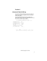
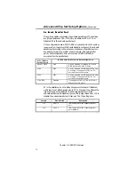
Page 73: ...lowing screen appears BIOS SETUP PROGRAM ADVANCED CHIP SET SETUP C 1991 American Megatrends 1990 All rights reserved On Board Serial Port 1 3f8 On Board Serial Port 2 2f8 On Board Parallel Port 378 On Board Floppy Controller Disabled On Board IDE Controller Disabled 8 bit DMA Active Clock 2 CLKs 16 bit DMA Active Clocks 2 CLKs DMA Clocks SCLK 2 Command Delay 8 bit Cycle No Command Delay 16 bit Cyc...

Page 74: ...nfigured as None 3F8h Can be disabled or changed to 3E8h via BIOS Advanced Chip Set Setup 3F8h 3E8h Can be disabled via BIOS Advanced Chip Set Setup If changed to 3F8h an I O port address conflict occurs 3E8h 3F8h Can be disabled via BIOS Advanced Chip Set Setup If changed to 3E8h an I O port address conflict occurs 3F8h 3E8h Disabled If changed to 3F8h or 3E8h an I O port address conflict occurs ...

Page 75: ...t 2 is Autoconfigured as None 2F8h Can be disabled or changed to 2E8h via BIOS Advanced Chip Set Setup 2F8h 2E8h Can be disabled via BIOS Advanced Chip Set Setup If changed to 2F8h an I O port address conflict occurs 2E8h 2F8h Can be disabled via BIOS Advanced Chip Set Setup If changed to 2E8h an I O port address conflict occurs 2F8h 2E8h Disabled If changed to 3F8h or 3E8h an I O port address con...

Page 76: ...oard Parallel Port is Autoconfigured as None or 3BCh 378h Can be disabled or changed to 278h via BIOS Advanced Chip Set Setup 378h 278h Can be disabled via BIOS Advanced Chip Set Setup If changed to 378h an I O port address conflict occurs 278h 378h Can be disabled via BIOS Advanced Chip Set Setup If changed to 278h an I O port address conflict occurs 378h 278h Disabled If changed to 378h or 278h ...

Page 77: ...he settings are Enabled or Disabled 8 b i t 8 b i t D M A A c t i v e C l o c k D M A A c t i v e C l o c k The settings are 2 3 or 4 CLKs This option sets the number of clock cycles the command is active for 8 bit DMA cycles 1 6 b i t D M A A c t i v e C l o c k 1 6 b i t D M A A c t i v e C l o c k The settings are 2 3 or 4 CLKs This option sets the number of clock cycles the command is active f...

Page 78: ...ion sets one extra command delay for 16 bit memory cycles The settings are Yes or No 8 b i t I O W a i t S t a t e s 8 b i t I O W a i t S t a t e s The PC AT compatible value is 4 wait states The settings are 4 wait states or 5 wait states 1 6 b i t I O W a i t S t a t e s 1 6 b i t I O W a i t S t a t e s The PC AT compatible setting is 0 wait states The settings are 0 or 1 wait states ...

Page 79: ... or whenever the end user runs Setup The password function can also be disabled If disabled the prompt does not appear Changing a Password The password check option is enabled in Advanced CMOS Setup Page 66 by choosing Always or Setup The password 1 6 characters is stored in CMOS RAM To change a password select the Change Password option from the main Setup screen and press Enter The following pro...

Page 80: ...in Advanced CMOS Setup he is prompted for the password U s i n g a P a s s w o r d U s i n g a P a s s w o r d The end user must enter the new password when the password prompt appears and then press Enter The end user should use the default password if CMOS RAM is corrupted The end user should keep a record of the new password when the password is changed If he forgets the password and password p...

Page 81: ...um interleave factor Page 80 Media Analysis Analyzes each hard disk drive track to determine whether it is usable The track is marked bad if unusable Page 82 Hard Disk Utility Error Messages Explanations of all error messages that can be generated by the Hard Disk Utilities Page 83 These routines work on drives that use the MFM RLL ARLL or ESDI data recording techniques They do not work on IDE or ...

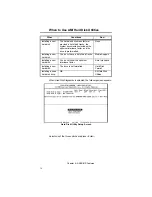
Page 82: ...formatted None Installing a new hard disk You do not have a list of bad tracks Media Analysis Installing a new hard disk You do not know the optimum interleave factor Auto Interleave Installing a new hard disk The drive is not formatted Hard Disk Format Installing a used hard disk drive N A All Hard Disk Utilities When Hard Disk Diagnostics is selected the following screen appears Select one of th...

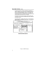
Page 83: ...t work on IDE or SCSI drives Use Hard Disk Format to integrate a new hard disk to the system or to reformat a used hard disk which has developed bad tracks as a result of aging or poor handling Select Media Analysis to find bad tracks When Enter is pressed at Hard Disk Format the following prompt appears Hard Disk Format Disk Drive C D Disk Drive Type Interleave 1 16 Mark Bad Tracks Y N Proceed Y ...

Page 84: ...isk Drive Type is read from CMOS RAM The Interleave factor can be selected manually or determined by Auto Interleave The hard disk drive manufacturer usually provides a list of bad tracks Enter these tracks They are then marked as bad to prevent data from being stored on them The following screen is displayed after entering Y in Mark Bad Tracks pressing Enter and selecting add delete revise or cle...

Page 85: ...owing warning prompt appears WARNING INFORMATION All Data on Specified Hard disk will be LOST Want to Continue Y N N Press Enter to return to the main Hard Disk Utility screen To proceed type Y and press Enter Warning Once you type Y and press Enter data on the hard drive is irrevocably lost ...

Page 86: ...ugh trial and error by measuring the transfer rate for four different interleave values To determine the best interleave factor the system formats a portion of the hard disk for each transfer rate calculated The cylinders heads and sectors formatted for each value is displayed in the activity box It does not work on IDE or SCSI drives Select Auto Interleave on the main Hard Disk Utility Screen and...

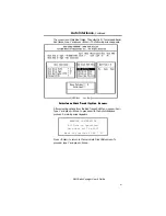
Page 87: ...c k O p t i o n S c r e e n I n t e r l e a v e B a d T r a c k O p t i o n S c r e e n After selecting options from the Bad Tracks Edit Menu press Esc Type Y and press Enter to proceed with the Auto Interleave process A warning screen appears WARNING INFORMATION All Data on Specified Hard disk will be LOST Want to Continue Y N N Press Enter to return to the main Hard Disk Utility screen To procee...

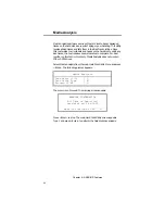
Page 88: ...s several minutes to complete For best results run this test in its entirety Media Analysis does not work on IDE or SCSI drives Select Media Analysis from the main Hard Disk Utility Menu and press Enter The following prompt appears Media Analysis Disk Drive C D Disk Drive Type Proceed Y N C 47 3 The cursor is on Proceed The warning screen appears WARNING INFORMATION All Data on Specified Hard disk...

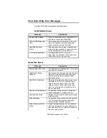
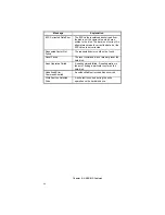
Page 89: ... Address Mark Not Found The address mark initial address on the hard disk could not be found Attachment Failed to Respond No response has been received from the hard disk drive An operation has already begun and the hard disk did not respond It had responded earlier Bad ECC on Disk Read When the hard disk drive utility writes it also calculates an ECC Error Correction Code value for the data being...

Page 90: ...value is not corrected Requested Sector Not Found The requested sector could not be found Reset Failed The reset command did not properly reset the hard disk Seek Operation Failed A seek command failed A seek operation is the act of finding a particular sector on the hard disk Undefined Error Command Aborted An unidentifiable error condition occurred Write Fault on Selected Drive A write fault occ...

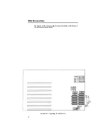
Page 91: ... should be 1 2 shorted 2 Place a jumper across J36 to implement 256K cache The positions should be J36 1 2 shorted 3 Remove the static RAM from U33 This RAM is not required for 256 KB cache operation 4 Remove the 22 pin 16 KB x 4 static RAM chips from U38 U39 U41 U42 U45 U46 U48 and U49 5 Place the 24 pin 64 KB x 4 static RAM chips in U38 U39 U41 U42 U45 U46 U48 and U49 Make sure that the pins are...

Page 92: ...Appendix A Upgrading Cache Memory 86 SRAM Locations The figures on the following graphic show the location of SRAMs and the jumpers discussed above ...

Page 93: ...terleave Utility 78 Baby Voyager Graphic 8 Base 64 KB Memory Failure 34 BIOS Beep Codes 34 Error Reporting 33 Fatal Errors 34 Hard Disk Utilities 73 Non Fatal Error Messages 35 Password Check 64 Password Support 71 POST Power On Self Test 33 BIOS Setup 42 Board Layout 8 C Drive Error 35 Cables 21 CMOS Display Type Mismatch 36 CMOS Shutdown Register Read Write Error 34 CMOS System Options Not Set 3...

Page 94: ...loppy Disk Drive 26 P7 IDE Hard Disk 28 PS2 Power Supply 19 PS3 Power Supply 19 Coprocessors Installing 16 Test 17 DMA 69 DMA Clocks 69 EGA Adapters 10 Fast Gate A20 63 Fast Gate A20 Options 63 Fixed Disk Drive Controller 69 Floppy Controller 69 Floppy Disk Connector Pinout 26 Floppy Drive 56 Floppy Drive connector Pinout 27 Formatting Hard Drive 75 Hard Disk 53 P7 IDE Hard Disk Connector 28 Hard ...

Page 95: ...ess 0 Wait State 11 Jumpers 10 11 J18 Parallel Port IRQ Select 11 J19 Burst Address 2 11 J20 Burst Address 3 11 J21 J22 Cache Address Select 12 J28 Bus Clock Select 11 J29 BIOS ROM Size Select 12 J35 Enable Burst Mode 11 J36 Cache Select 12 J4 J5 Memory Configuration 10 13 J6 COM2 IRQ Select 11 J9 COM1 IRQ Select 10 Keyboard J3 Connector 20 Lock Connector 22 Layout 8 Manufacturing Test Port 33 Mar...

Page 96: ...E Hard Disk Connector 28 Onboard Adapters P5 Parallel Port 25 Parallel Port 25 68 Pinout 25 Pinout Adapter Cards 29 Floppy connector 27 Parallel Port 25 Serial ports 24 POST Memory Test 42 Power Supply 19 Processor error 34 Reset Button Connector 21 Serial Port 23 66 Connectors 24 Pinout 24 Serial Port 2 67 Serial Port Pinouts 24 Setup 42 Above 1 MB Memory Test 60 Auto Configuration 49 Auto Config...

Page 97: ...MOS Setup 51 System Boot Up CPU Speed 63 System Boot Up Num Lock 62 System Boot Up Sequence 62 Typematic Rate 59 Typematic Rate and Delay 59 Typematic Rate Delay and Typematic Rate 59 Video or Adaptor ROM Shadow 64 Warning Message 48 warning screen 58 SIMMs 13 Installing 15 Part numbers 14 Speaker Cable Connector 22 Specifications 2 SW1 10 Switch and Jumper Options 10 Switches SW1 10 Testing Syste...

Reviews: