
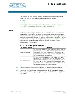


8–6
Chapter 8: Reset and Clocks
Clocks
Stratix V Hard IP for PCI Express
June 2012
Altera Corporation
■
■
■
p_clk
The transceiver derives
p_clk
from the 100 MHz
refclk
signal that you must provide
to the device. The
PCI Express Base Specification 2.1
requires that the
refclk
signal
frequency be 100 MHz
±
300 PPM; however, as a convenience, you can also use a
reference clock that is 125 MHz
±
300 PPM.
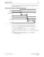
The transitions between Gen1, Gen2, and Gen3 should be glitchless.
p_clk
can be
turned off for most of the 1 ms timeout assigned for the PHY to change the clock rate;
however,
p_clk
should be stable before the 1 ms timeout expires.
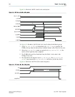
The CDC module implements the asynchronous clock domain crossing between the
PHY/MAC
p_clk
domain and the Data Link Layer
coreclk
domain. The transceiver
p_clk
clock is connected directly to the Hard IP for PCI Express and does not connect
to the FPGA fabric.
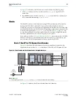
coreclkout
The
coreclkout_hip
signal is derived from
p_clk
lists frequencies for
coreclkout_hip
, which are a function of the link width, data rate, and the width of the
Avalon-ST bus.
The frequencies and widths specified in
are maintained throughout
operation. If the link downtrains to a lesser link width or changes to a different
maximum link rate, it maintains the frequencies it was originally configured for as
specified in
. (The Hard IP throttles the interface to achieve a lower
throughput.)
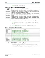
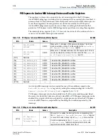
Table 8–2. coreclkout_hip Values for All Parameterizations
Link Width
Max Link Rate
coreclkout_hip
×1
Gen1 64
125
MHz
×1
Gen1
64
62.5 MHz
×4
Gen1 64
125
MHz
×8
Gen1 64
250
MHz
×8
Gen1
128
125 MHz
×1
Gen2
64
125 MHz
×4
Gen2
64
250 MHz
×4
Gen2
128
125 MHz
×8
Gen2
128
250 MHz
×8
Gen2
256
125 MHz
×1
Gen3
64
125 MHz
×4
Gen3
128
250 MHz
×4
Gen3
256
125 MHz