background image

Function groups 15

Manual ADQ-22/23-Serie Rev. 1.1 

Function groups

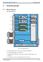
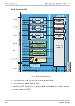
Block diagram ADQ-23

ADQ-23

DO_E7…0

DIO_G7…0

GND_EXT

DI_A7…0

GND_EXT

VEXT_DO

GND_PC

VCC_OUT (+5 V)

DI Port C

GND_EXT

VEXT_DI

DI_B7…0

IRQ

DO_F7…0

GND_EXT

VEXT_DO

IRQ

DI Port A

DI Port B

DO Port E

DO Port F

Relay Port D

DIO Port G

GND_EXT

DI_C7…0

CO_x

NO_x

NC_x

IDC connector

78-pin D-Sub female connector

Address-/

data bus

CompactPCI Serial       /       PCI Express interface

Molex connector

(+5V for PCI Express)

Interrupt

Control and 

interrupt logic 

Temperature monitoring

Temperature monitoring

TTL-I/Os

(1 x 8 bit port)

Current limitation per channel

Current limitation per channel

Isolated up to 500 V

IRQ

Bit-pattern match

Bit-pattern change

8 bit digital input

IRQ

Bit-pattern match

Bit-pattern change

8 bit digital input

IRQ

Bit-pattern match

Bit-pattern change

8 bit digital input

Digital

filter

Digital

filter

Digital

filter

8 bit output port

8 bit output port

8 bit input port

8 bit input port

8 bit input port

Fig. 4:  Block diagram ADQ-23

•  24 isolated digital inputs (3 x 8 bit ports) with programmable filter

•  16 isolated digital outputs (2 x 8 bit ports)

•  8 bidirectional TTL digital I/Os (1 x 8 bit port) usable via supplied adapter cable if required

•  8 change-over relays (SPDT)

3.2  Isolated digital inputs

The 

ADQ-22

 has 2 isolated digital input ports with 16 bits each and the 

ADQ-23

 has 3 isolated 

digital input ports with 8 bits each. The isolated inputs have a Schmitt trigger characteristic 
according to IEC 61131-2 (type 1) and are designed for a max. input voltage of 35 V. All isolated 
inputs are equipped with status LEDs. The isolation voltage against PC ground is 500 VACeff 
according to EN60664-1 or UL1577. 

If required, all inputs can be monitored for bit change or bit pattern equality and evaluated as 
an interrupt event. In addition, an interrupt can be triggered if the external voltage supply is too 
low (VEXT_DI < 8 V) or missing (VEXT_DI < 12.1 V).

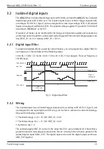
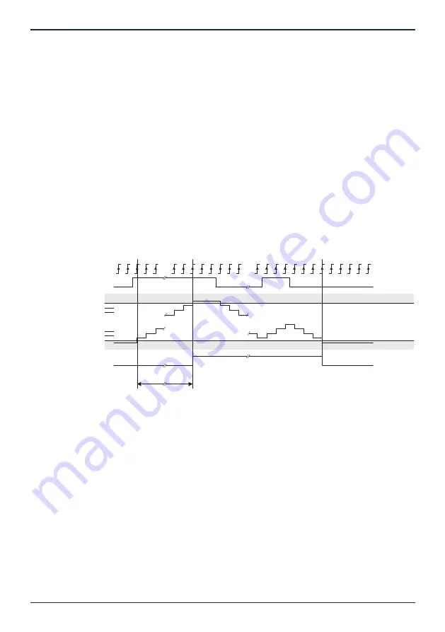
3.2.1  Digital input filter

To prevent unwanted effects caused by contact bounce, you can programme a digital filter for 
each input port. Choose between the following values: 

10 ms (N = 1248) / 3.2 ms (N = 400) / 1.0 ms (N = 125) / 10 µs (bypass). The scan frequency is 
100 kHz (typ.). 

0

1

2

N-1

N-2

N-3

Scan frequency

Input DI_x

Filter output

Filter state

Signal is 1

Signal is 0

Filter time

Signal is

unchanged

Fig. 5:  Digital input filter

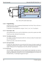
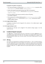
3.2.2  Wiring 

The isolated inputs have a Schmitt trigger characteristic according to IEC 61131-2 (type 1) and 
are designed for the input high level UIH of typ. 24 V which is common in control technology. 
Observe the following conditions: 

•  Threshold voltage L x H: > 15 V @ VEXT_DI = 24 V

•  Threshold voltage H x L: < 11 V @ VEXT_DI = 24 V

•  Hysteresis: typ. 1 V

The external supply VEXT_DI can be in the range 9.6..35 V, we recommend 24 V. Note that a 
ground connection must always be made from the ext. circuitry to the reference ground of the 
isolated digital inputs (GND_EXT). The digital input section and the digital output section use 
GND_EXT together. 

Summary of Contents for ADQ-22 PCIe

Page 1: ...Manual Rev 1 1 EN ADQ 22 23 PXI PXIe PCIe Digital I O boards with up to 32 isolated digital inputs up to 32 isolated digital outputs 16 TTL digital I Os ADQ LINK optional 8 change over relays...

Page 2: ...rt E Mail support alldaq com Phone 49 0 89 894 222 74 Fax 49 0 89 894 222 33 Internet www alldaq com support Copyright 2015 ALLNET GmbH Computersysteme All rights reserved All information contained in...

Page 3: ...3 Test programme 10 2 4 ALLDAQ Manager 10 3 Function groups 13 3 1 Block diagrams 13 3 2 Isolated digital inputs 15 3 2 1 Digital input filter 15 3 2 2 Wiring 15 3 2 3 Programming 16 3 2 3 1 Easy read...

Page 4: ...n assignments 27 4 2 1ADQ 22 27 4 2 1 1 78 pin Sub D socket ST1 27 4 2 1 2 25 pin Sub D socket ST2 28 4 2 1 3 25 pin Sub D socket ADQ LINK 28 4 2 2 ADQ 23 29 4 2 2 1 78 pin Sub D socket ST1 29 4 2 2 2...

Page 5: ...on the unit You must never operate the appliance if it is damaged If in doubt contact our technical cus tomer service Please read this manual carefully before installing the unit 1 1 Scope of deliver...

Page 6: ...rised personnel When commissioning the unit please observe the installation regulations and all relevant standards incl VDE standards especially when operating with voltages greater than 42 V We recom...

Page 7: ...ffectively suppresses interference To protect against contact bounce these cards also offer the option of programming a digital filter per input port Streaming operation enables continuous polling of...

Page 8: ...Included with the card is a Plug Play driver for Windows Microsoft and higher 32 and 64 bit as well as a function library API with code examples for high level language programming Please note the in...

Page 9: ...ystem Open the housing as described in the manual of your PC system Make sure that no static discharge can take place via the card when it is inserted At least one hand should be earthed to discharge...

Page 10: ...applies Start the menu guided installation of the ALLDAQ driver by executing the ALLDAQDriverSe tup64 exe or 32 exe in the target directory of your download After successful installation you will find...

Page 11: ...usually in the bottom right hand corner ALLDAQ Manager at a glance Information about the installed ALLDAQ hardware at a glance XML export of the driver configuration for archiving and support Tool fo...

Page 12: ...12 Function groups Function groups Manual ADQ 22 23 Serie Rev 1 1...

Page 13: ...n Bit pattern change 16 bit digital input IRQ Bit pattern comparison Bit pattern change 16 bit digital input Temperature monitoring Temperature monitoring TTL I Os 2 x 8 bit port Current limit per cha...

Page 14: ...itoring Temperature monitoring TTL I Os 1 x 8 bit port Current limitation per channel Current limitation per channel Isolated up to 500 V IRQ Bit pattern match Bit pattern change 8 bit digital input I...

Page 15: ...ffects caused by contact bounce you can programme a digital filter for each input port Choose between the following values 10 ms N 1248 3 2 ms N 400 1 0 ms N 125 10 s bypass The scan frequency is 100...

Page 16: ...es the continuous reading of the digital inputs up to 1 kS s port by port Follow the procedure as described in the online help 3 2 3 3 Interrupt modes If required the isolated input ports can be monit...

Page 17: ...e RisingEdge 04Hex An interrupt is triggered as soon as a rising edge arrives at bit b2 The interrupt event is evaluated with the parameters uiPortBitChangeRisingEdge or uiPortBitChangeFallingEdge of...

Page 18: ...rupt can be triggered in the absence of an external power supply VEXT_DI 12 1 V 3 2 3 3 4 Supply voltage too low If necessary an interrupt can be triggered if the external voltage supply is too low VE...

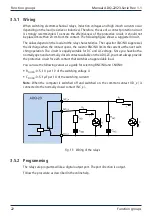
Page 19: ...utomatic restart In case of overload TTSD typ 135 C the respective channel switches off and switches on again automatically as soon as the junction temperature has dropped by 10 K In the event of an o...

Page 20: ...ned is automatically switched off and an interrupt is generated Observe the procedure as described in the online help 3 4 Bidirectional digital inputs outputs The ADQ 22 series has a bidirectional 16...

Page 21: ...ow the procedure as described in the online help 3 4 2 2 Streaming operation Depending on the port direction the software controlled streaming operation enables the con tinuous reading of the digital...

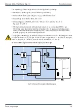
Page 22: ...r RNC NO limits the current at the next swit ching operation The circuit is equally suitable for DC and AC voltage Since you have both a normally open and a normally closed contact available on the AD...

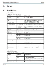
Page 23: ...1 V hysteresis typ 1 V Input current VEXT_DI 24V min 2 3 mA per channel Status LEDs per channel Input filter programmable per port Filter off bypass typ 10 s N 1 Filter time 1 typ 1ms N 125 Filter tim...

Page 24: ...toff switch off time RL 47 up to 10 UO typ 89 s max 170 s dUO dt on slope when switching on von 10 30 UO RL 47 VEXT_DO 15V typ 1V s max 2V s dUO dt off slope when switching off from 70 40 UO RL 47 VEX...

Page 25: ...mA min 2 4V UOL IO 24mA max 0 5V IO 24mA Streaming operation per channel max 1kS s via software timer General Element Condition Specification PC interface depending on model PXIe models PXIe Serial Re...

Page 26: ...ls 78 pin Sub D socket ST1 25 pin Sub D socket ST2 via additional slot plate PCIe models 78 pin Sub D socket ST1 25 pole Sub D socket ST2 via additional slot plate Molex connector 5 V Certifications E...

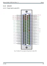
Page 27: ...4 DO_D6 53 DO_D5 52 DO_D4 51 DO_D3 50 DO_D2 49 DO_D1 48 DO_D0 47 DI_B7 46 DI_B6 45 DI_B5 44 DI_B4 43 DI_B3 42 DI_B2 41 DI_B1 40 DI_B0 39 VEXT_DO 38 VEXT_DO 37 VEXT_DO 36 DO_C8 35 DO_C9 34 DO_C10 33 DO...

Page 28: ...ment 25 pin Sub D socket left and pin connector strip ST2 right 4 2 1 3 25 pin Sub D socket ADQ LINK 1 2 ADQ LINK GND PC 3 4 GND PC 5 6 GND PC 7 8 GND PC 9 10 GND PC 11 12 GND PC 13 14 GND PC 15 16 GN...

Page 29: ...54 DO_E6 53 DO_E5 52 DO_E4 51 DO_E3 50 DO_E2 49 DO_E1 48 DO_E0 47 DI_B7 46 DI_B6 45 DI_B5 44 DI_B4 43 DI_B3 42 DI_B2 41 DI_B1 40 DI_B0 39 VEXT_DO 38 VEXT_DO 37 VEXT_DO 36 NC_1 35 NO_1 34 NC_2 33 NC_3...

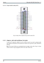
Page 30: ...GND_PC 1 VCC_OUT Fig 16 ADQ 23 Pin assignment 25 pin Sub D socket ST2 4 2 3 Adapter cable with additional slot plate To use the TTL digital I Os ADQ 22 port E or ADQ 23 port G you need an adapter cab...

Page 31: ...ale connector strip 20 or 26 pole socket connector Fig 17 Additional slot plate panel Connection adapter cable with slot bracket ADQ 22 PXIE ADQ 22 23 PCIe 1 1 1 1 Female connector 20 pole Fig 18 Conn...

Page 32: ...the scope of delivery of ADQ 22 23 cPCIS CompactPCI cover 4TE with 25 pin Sub D socket on 20 pin socket strip ADQ AP D25F PCI Art No 111756 included in the scope of delivery of ADQ 22 23 PCIe PCI slot...

Page 33: ...s power supply units etc ALLNET products are manufactured in compliance with RoHS Restriction of the use of certain hazardous substances 4 5 3 CE marking The ADQ 22 23 series carries the CE marking Th...

Page 34: ...d inputs 13 Functional groups 11 I Important notes 31 Initial operation 9 Installation 10 Introduction 5 M MOLEX connector 9 Mounting 6 P Pinout 25 pin D Sub connector ST2 26 28 78 pin D Sub connector...

Page 35: ...Annex 35 Manual ADQ 22 23 Serie Rev 1 1 Annex W Warranty 31 Wiring Isolated digital inputs 13 Isolated digital outputs 16 Relays 20 TTL digital I Os 18...

Page 36: ...ALLNET GmbH Computersysteme Division ALLDAQ Maistrasse 2 D 82110 Germering E Mail support alldaq com Phone 49 0 89 894 222 74 Fax 49 0 89 894 222 33 Internet www alldaq com...

Reviews: