


FPGA Video Processing Development Platform AV6150 User Manual
40 / 55
Contact Email: [email protected]
The RTL8211EG chip supports 10/100/1000 Mbps network transmission rate
and communicates with the FPGA through the GMII interface. RTL8211EG
supports MDI/MDX adaptive, various speed adaptations, Master/Slave
adaptation, and support for MDIO bus for PHY register management.
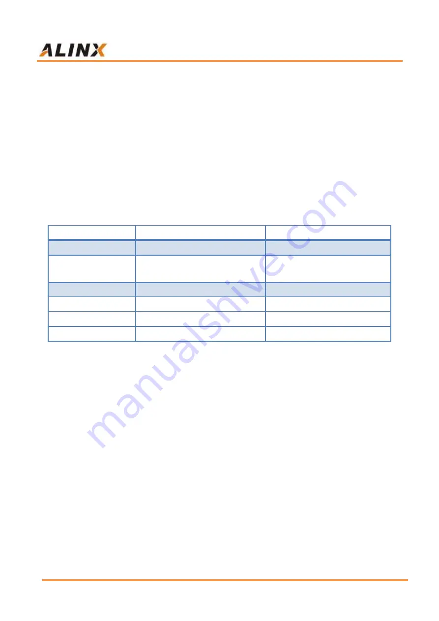
The RTL8211EG will detect the level status of some specific IOs to
determine their working mode after powered on. Table 4-6-1 describes the
default setup information after the GPHY chip is powered on.
Configuration Pin
Instructions
Configuration value
PHYAD[2:0]
MDIO/MDC Mode PHY Address
PHY Address 011
SELRGV
3.3V, 2.5V, 1.5/1.8V voltage
selection
3.3V
AN[1:0]
Auto-negotiation configuration
(10/100/1000M) adaptive
RX Delay
RX clock 2ns delay
Delay
TX Delay
TX clock 2ns delay
Delay
Mode
RGMII or GMII selection
RGMII
Table 4-6-1: PHY chip default configuration value
When the network is connected to Gigabit Ethernet, the data
transmission of FPGA and PHY chip RTL8211EG is communicated through the
RGMII bus, the transmission clock is 125Mhz. The receive clock E_RXC is
provided by the PHY chip, the transmit clock E_GTXC is provided by the FPGA,
and the data is sampled on the rising edge of the clock.
When the network is connected to 100M Ethernet, the data transmission of
FPGA and PHY chip RTL8211EG is communicated through the GMII bus, the
transmission clock is 25Mhz. The receive clock E_RXC is provided by the PHY
chip, the transmit clock E_GTXC is provided by the FPGA, and the data is
sampled on the rising edge of the clock.