


[AK4675]
MS0963-E-00
2008/05
- 33 -
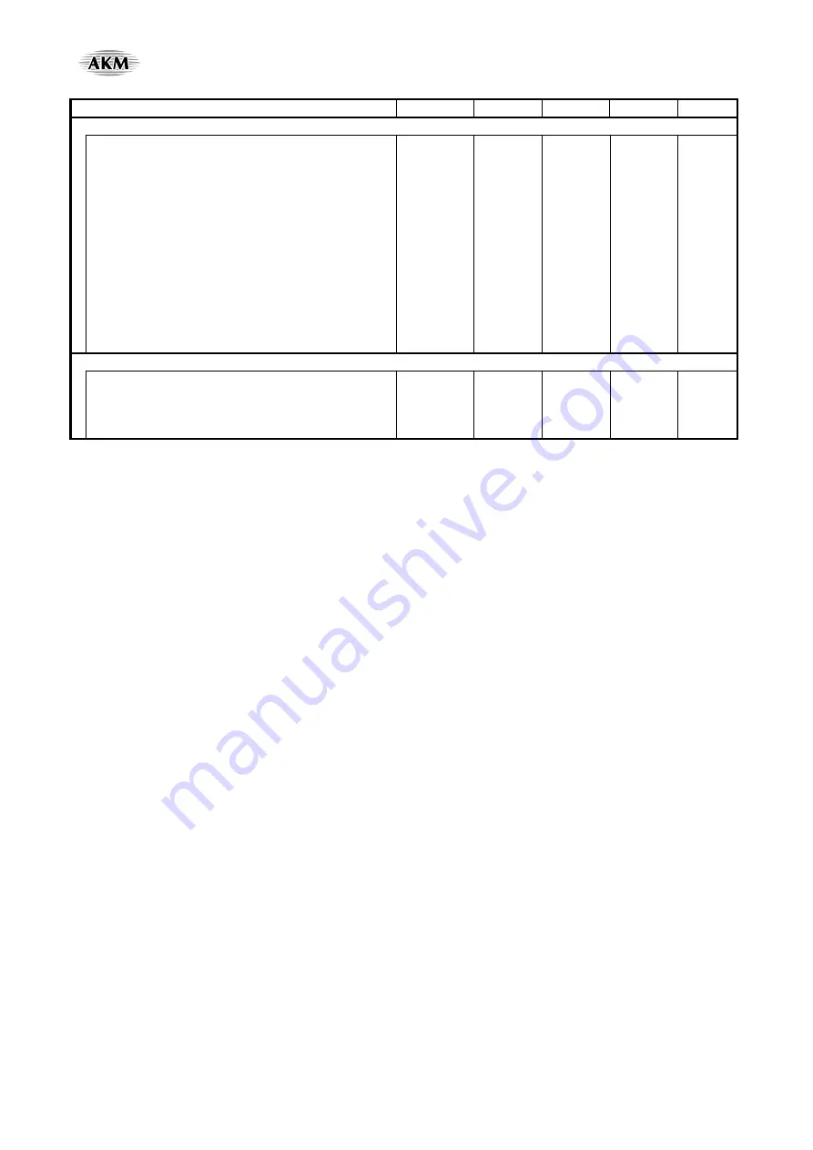
Parameter Symbol
min
typ
max
Units
Control Interface Timing (I
2
C Bus mode):
)
SCL Clock Frequency (
fSCL 30 - 400
kHz
Bus Free Time Between Transmissions
tBUF 1.3 -
-
μ
s
Start Condition Hold Time (prior to first clock pulse)
tHD:STA
0.6
-
-
μ
s
Clock Low Time
tLOW
1.3
-
-
μ
s
Clock High Time
tHIGH
0.6
-
-
μ
s
Setup Time for Repeated Start Condition
tSU:STA
0.6
-
-
μ
s
SDA Hold Time from SCL Falling (
) tHD:DAT
0 - -
μ
s
SDA Setup Time from SCL Rising
tSU:DAT
0.1
-
-
μ
s
Rise Time of Both SDA and SCL Lines
tR
-
-
0.3
μ
s
Fall Time of Both SDA and SCL Lines
tF
-
-
0.3
μ
s
Setup Time for Stop Condition
tSU:STO
0.6
-
-
μ
s
Capacitive Load on Bus
Cb
-
-
400
pF
Pulse Width of Spike Noise Suppressed by Input Filter
tSP
0
-
50
ns
Power-down & Reset Timing
PDN Pulse Width (
)
tPD 150 - - ns
PMADL or PMADR “
↑
” to SDTO valid (
tPDV - 1059 - 1/fs
PMSRA “
↑
” to SDTOA valid (
)
tPDV2 - 21 - 1/fs2
PMSRB “
↑
” to SDTO valid (
)
tPDV3 - 135 - 1/fs
Note 69. I
2
C is a registered trademark of Philips Semiconductors.
Note 70. In case that SAR ADC data is read out via I
2
C bus, SCL should be input corresponding 2 byte data including
ACK (
).
Note 71. Data must be held long enough to bridge the 300ns-transition time of SCL.
Note 72. CODEC & SRC blocks of the AK4675 can be reset by bringing PDN pin = “L” to “H” only upon power up
Note 73. This is the count of LRCK “
↑
” from the PMADL or PMADR bit = “1” when PMSRB bit = “0”.
Note 74. The signal path is SDTI
→
SRC-A
→
SDTOA and PLLBT is locked.
Note 75. The signal path is SDTIA
→
SRC-B
→
SDTO.


