ASAHI KASEI
[AKD4584]
<KM065802>
2009/06
- 8 -
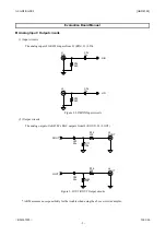
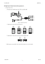
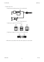
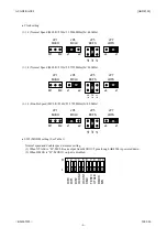
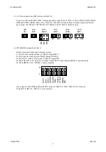
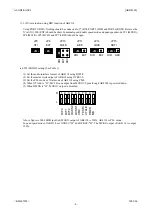
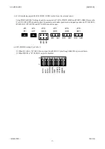
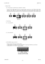
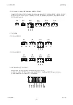
(1-3) D/A evaluation using DIR function of AK4114
Using PORT1 (DIR). Nothing should be connected to J7 (RX), PORT5 (DIR) and PORT6 (ROM). Remove the
X’tal (X1). JP6 (EXT) should be short. In normal speed, double speed mode and quad speed mode, JP1 (MCKO),
JP4 (MCLK), JP5 (BCFS) and JP7 (LRFS) should be open.
JP10
MCLK
JP3
XTI
JP14
LRCK
JP6
EXT
JP11
BICK
EXT
DIR
DI
R
EXT
AD
C
JP15
SDTI
ADC
DIR
EXT
DIR
•
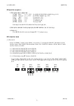
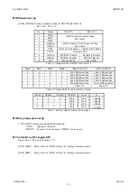
SW2 (MODE) setting (See Table 1)
(1)
Set the audio interface format of AK4114 using DIF2-0.
(2)
Set the master clock output of AK4114using OCKS1-0.
(3)
Set the PLL mode or X’tal mode of AK4114 using CM0.
(4)
When XTALE is “H”, MCLK can output from MCKO1/2 pins though AK4584 is powered down.
(5)
When DMCK is “H”, MCKO1 output is disabled.
H
L
1 2 3 4 5
8
6 7
9 10
DI
F
0
DI
F
1
DI
F
2
O
C
KS0
O
C
KS1
CM
0
TES
T
3
XT
A
L
E
DM
CK
MS
Above figure is 24bit MSB justified, MCKO output of AK4114 is 256fs, AK4114 is PLL mode.
In quad speed mode of AK4114, set OCKS1=“H” and OCKS0=“H”. The MCKO output of AK4114 is output
128fs.


