background image

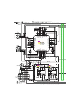
WIRING – 3  (AMP  1F)

32

31

30

29

28

27

26

25

24

23

22

21

20

19

18

17

16

15

14

13

12

11

10

9

8

7

6

5

4

3

2

1

– 21 –

A

B

C

D

E

F

G

H

I

J

K

L

M

N

O

P

Q

R

S

T

U

All manuals and user guides at all-guides.com

all-guides.com

Summary of Contents for XR-DV526

Page 1: ...AAPA XR DV526 U S M Code No 09 00A 434 1R1 If requiring information about the DVD mechanism see Service Manual of AZG D S M Code No 09 00A 350 6N2 SPEAKERS SX WNDV526 SX R275 SX C605 This Service Manual is the Revision Publishing and replaces Simple Manual S M Code No 09 007 434 1T1 R E V I S I O N All manuals and user guides at all guides com a l l g u i d e s c o m ...

Page 2: ...ingle sided single layer single sided double layer double sided double layer 8 cm single sided single layer single sided double layer double sided double layer Compact discs CD DA CD R CD RW video CD 12 cm and 8 cm discs S VIDEO OUT Y output 1 Vp p 75 ohms sync negative C output 0 286 Vp p VIDEO OUT Video composit output 1 Vp p 75 ohms sync negative One RCA jack Operating conditions 5 C to 35 C 41...

Page 3: ...änsen för laserklass 1 PROTECTION OF EYES FROM LASER BEAM DURING SERVICING CAUTION Use of controls or adjustments or performance of proce dures other than those specified herin may result in hazardous radiation exposure ATTENTION L utillisation de commandes réglages ou procédures autres que ceux spécifiés peut entraîner une dangereuse exposition aux radiations ADVARSEL Usynliglaserstålingvedåbning...

Page 4: ...irm that the main power is turned on and the HOLD terminal of the MICROCOMPUTER keeps the H level or not 3 3 3 3 3 When the HOLD terminal is L level the abnormality detection circuit is judged to be working correctly and the MICROCOMPUTER is judged to be good 1 Forced discharge of electrolytic capacitor of power supply block When repair is going to be attempted in the set that uses relay circuit i...

Page 5: ...ic capacitor C113 that is connected to VDD of the MICROCOMPUTER with tweezers 3 3 3 3 3 Connect the AC power cord again If the MICROCOMPUTER returns to the normal operation the MICROCOMPUTER is good Note The reference number or MICROCOMPUTER pin number of transistor Q110 and electrolytic capacitor C113 can change depending on the models Be sure to check the reference numbers on schematic diagram b...

Page 6: ...0V C34 87 010 260 080 CAP ELECT 47 25V C35 87 010 380 080 CAP ELECT 47 16V C36 87 010 381 080 CAP ELECT 330 16V C38 87 010 409 080 CAP E 220 50 SME C39 87 010 409 080 CAP E 220 50 SME C40 87 010 197 080 CAP CHIP 0 01 DM C60 87 010 403 080 CAP ELECT 3 3 50V C80 87 010 401 080 CAP ELECT 1 50V C81 87 010 383 080 CAP ELECT 33 25V C82 87 010 260 080 CAP ELECT 47 25V C104 87 010 196 080 CHIP CAPACITOR 0...

Page 7: ... C461 87 010 196 080 CHIP CAPACITOR 0 1 25 C463 87 010 196 080 CHIP CAPACITOR 0 1 25 C465 87 016 669 080 C CAP S 0 1 25 C466 87 010 194 080 CAP CHIP 0 047 C467 87 A10 201 080 C CAP S 0 33 16 K B C468 87 A10 060 080 C CAP S 0 18 16 K B C472 87 012 140 080 C CAP S 470P C473 87 012 140 080 C CAP S 470P C474 87 012 140 080 C CAP S 470P C475 87 012 140 080 C CAP S 470P C476 87 012 140 080 C CAP S 470P ...

Page 8: ... CN1 87 A60 996 010 CONN 13P V BLK TAC L13X A3 CN91 87 A60 109 010 CONN 2P V S2M 2W CN101 87 A60 996 010 CONN 13P V BLK TAC L13X A3 CN301 87 099 827 010 CONN 3P S2M 3W CN351 87 099 832 010 CONN 8P S2M 8W CN431 87 099 013 010 CONN 11P 6216 V CN601 87 099 719 010 CONN 30P TYK B X CN610 87 A61 171 010 CONN 5P V GRY FMN BTK CN611 87 049 919 010 CONN 3P EH V WHT CNA1 8A NF8 653 010 CONN ASSY 9P TID A 4...

Page 9: ...11BT S419 87 A91 024 180 SW TACT KSHG611BT S425 87 A91 024 180 SW TACT KSHG611BT S426 87 A91 024 180 SW TACT KSHG611BT S427 87 A91 024 180 SW TACT KSHG611BT S428 87 A91 024 180 SW TACT KSHG611BT S429 87 A91 024 180 SW TACT KSHG611BT S430 87 A91 024 180 SW TACT KSHG611BT S431 87 A91 024 180 SW TACT KSHG611BT S432 87 A91 024 180 SW TACT KSHG611BT S433 87 A91 024 180 SW TACT KSHG611BT S434 87 A91 024...

Page 10: ...TID A CN102 87 099 198 010 CONN 10P 6216 V J101 87 A61 159 010 JACK PIN 4P R W B 0 KM L151 87 A50 610 010 COIL 1UH K MDEC L152 87 A50 610 010 COIL 1UH K MDEC L251 87 A50 610 010 COIL 1UH K MDEC R131 87 A00 258 080 RES M F 0 22 1W J R132 87 A00 258 080 RES M F 0 22 1W J R218 87 A00 258 080 RES M F 0 22 1W J TH201 87 A91 042 080 C THMS 100K 55001 PT C B C1 87 010 387 080 CAP E 470 25 SME C4 87 A11 1...

Page 11: ...p Resistor Part Coding Figure Value of resistor Chip resistor Wattage Type Tolerance 1 16W 1 10W 1 8W 1608 2125 3216 5 5 5 CJ CJ CJ Form L W t 1 6 0 8 0 45 2 1 25 0 45 3 2 1 6 108 118 128 A A CHIP RESISTOR PART CODE 0 55 Resistor Code Dimensions mm Symbol 1 16W 1005 5 CJ 1 0 0 5 0 35 104 L t W DTC144EK RT1N141C RT1P141C RT1P144C RT1P441C DTC114ES KTC3199 E C B All manuals and user guides at all gu...

Page 12: ... 12 BLOCK DIAGRAM 1 MAIN UNIT DVD UNIT All manuals and user guides at all guides com ...

Page 13: ... 13 BLOCK DIAGRAM 2 MAIN FRONT AMP 1F AMP PROLOGIC PT DECK All manuals and user guides at all guides com ...

Page 14: ...WIRING 1 MAIN VM 32 31 30 29 28 27 26 25 24 23 22 21 20 19 18 17 16 15 14 13 12 11 10 9 8 7 6 5 4 3 2 1 14 A B C D E F G H I J K L M N O P Q R S T U All manuals and user guides at all guides com ...

Page 15: ... 15 SCHEMATIC DIAGRAM 1 MAIN 1 4 VM All manuals and user guides at all guides com ...

Page 16: ... 16 SCHEMATIC DIAGRAM 2 MAIN 2 4 TUNER SECTION All manuals and user guides at all guides com a l l g u i d e s c o m ...

Page 17: ... 17 SCHEMATIC DIAGRAM 3 MAIN 3 4 DECK SECTION All manuals and user guides at all guides com ...

Page 18: ... 18 SCHEMATIC DIAGRAM 4 MAIN 4 4 PRO LOGIC SECTION All manuals and user guides at all guides com ...

Page 19: ...WIRING 2 FRONT 32 31 30 29 28 27 26 25 24 23 22 21 20 19 18 17 16 15 14 13 12 11 10 9 8 7 6 5 4 3 2 1 19 A B C D E F G H I J K L M N O P Q R S T U All manuals and user guides at all guides com ...

Page 20: ... 20 SCHEMATIC DIAGRAM 5 FRONT DECK All manuals and user guides at all guides com ...

Page 21: ... AMP 1F 32 31 30 29 28 27 26 25 24 23 22 21 20 19 18 17 16 15 14 13 12 11 10 9 8 7 6 5 4 3 2 1 21 A B C D E F G H I J K L M N O P Q R S T U All manuals and user guides at all guides com a l l g u i d e s c o m ...

Page 22: ... 22 SCHEMATIC DIAGRAM 6 AMP 1F All manuals and user guides at all guides com ...

Page 23: ...WIRING 4 AMP PROLOGIC 32 31 30 29 28 27 26 25 24 23 22 21 20 19 18 17 16 15 14 13 12 11 10 9 8 7 6 5 4 3 2 1 23 A B C D E F G H I J K L M N O P Q R S T U All manuals and user guides at all guides com ...

Page 24: ... 24 SCHEMATIC DIAGRAM 7 AMP PROLOGIC All manuals and user guides at all guides com ...

Page 25: ...WIRING 5 PT 15 14 13 12 11 10 9 8 7 6 5 4 3 2 1 A B C D E F G H I J K L M N O P Q R S T U 25 All manuals and user guides at all guides com ...

Page 26: ... 26 SCHEMATIC DIAGRAM 8 PT All manuals and user guides at all guides com a l l g u i d e s c o m ...

Page 27: ...23 22 21 20 19 18 17 16 15 14 13 12 11 10 9 8 7 6 5 4 3 2 1 27 A B C D E F G H I J K L M N O P Q R S T U WIRING 6 DECK G DECK C B 1 3 5 7 9 11 2 4 6 8 10 FFC302 TO FRONT C B CN302 W1 All manuals and user guides at all guides com ...

Page 28: ... 28 FL HNA 11MM34 GRID ASSIGNMENT ANODE CONNECTION PIN CONNECTION GRID ASSIGNMENT ANODE CONNECTION PIN CONNECTION All manuals and user guides at all guides com ...

Page 29: ... 29 IC BLOCK DIAGRAM All manuals and user guides at all guides com ...

Page 30: ... 30 All manuals and user guides at all guides com ...

Page 31: ...I DVD Mecha detect switch 24 I SPEANA I Spectrum analyzer signal input 25 NC Not connected 26 I RE VOL I Rotary encoder volume input 27 I RDS CLK I RDS clock input Not used 28 I TM BASE I Reference signal for clock 29 I RMC I Remote control signal input 30 40 G11 G1 O FL grid output 41 NC Not connected 42 45 P35 P32 O FL segment output 46 VDD3 Power supply 47 48 P31 P30 O FL segment output 49 P29 ...

Page 32: ...I FL segment output Deck 2 side A record switch data input 72 VDD4 Power supply 73 P7 I REV2 O I FL segment output Deck 2 reverse switch data input not used 74 P6 I REV1 O I FL segment output Deck 1 reverse switch data input not used 75 P5 NO ECO O I FL segment output NO ECO initial diode setting input not used 76 79 P4 P1 O FL segment output 80 O DVD CLOSE O DVD tray close output 81 O DVD OPEN O ...

Page 33: ...ND 3 BAND 3 BAND AM FM LW MW FM MW SW FM H L H H L H L L Outputs L or H as follows 10 MW SW O 2 BAND 3 BAND 3 BAND AM FM LW MW FM MW SW FM L L H L L L H L 11 IF MUTE O To control internal counter 12 IF IN I General purpose counter input 13 TUNE I Receives L when station is tuned 14 NC Not connected 15 AM IN I Receives the AM local oscillator frequency signal 16 FM IN I Receives the FM local oscill...

Page 34: ... 9dBµV 7 DC Balance Mono Distortion Adjustment Settings Test point TP3 TP4 DC Adjustment location L801 Input level 60dBµV Method Set to FM 98 0MHz and adjust L801 so that the voltage between TP3 and TP4 becomes 0V 300mV with distortion less than 1 3 8 Output Level Check AM Settings Test point TP8 Lch TP9 Rch Input level 74dBµV Method Set to AM 1000kHz and check that the test point is 74mV 3dB FM S...

Page 35: ...is 0dB 5dB 4 PB Sensitivity Check DECK 1 DECK 2 Settings Test tape TTA 200 Test point TP8 Lch TP9 Rch Method Play back the test tape and check that the output level of the test point is 230mV 3dB 5 REC PB Frequency Response Adjustment DECK 2 Settings Test tape TTA 602 Test point TP8 Lch TP9 Rch Input signal 1kHz 8kHz 20VU Adjustment location SFR351 Lch SFR352 Rch Method Apply a 1kHz signal and REC...

Page 36: ...s activated S M will display on the FL display tube S indicates the status M indicates the type of media Status indication Contents S41 Status that pickup stops at the inner circumference S42 Status that pickup stops at the inner circumterence with resume data S43 PLAY status S44 PAUSE status S45 SKIP status S46 TOC is being read S47 Signal of EEPROM writing end S48 Status in which status is not d...

Page 37: ...3 44 11 45 46 47 48 49 50 56 55 51 52 53 54 BINDER WIRE D D D D A A A A B G G A A A A C A J J A A H I A A A A D E E A F A A A A A A A A A AZG D ZAAPA PWB PWB K C FL401 PWB PLATE EARTH MIC PLATE EARTH MECH ZZM 3 YPR1NF CHAS MAIN AJ PLATE PT PT1 PWB PWB PWB PWB HT SINK VM2 HT SINK T5A P16 a a PLATE SHLD ASSY I A All manuals and user guides at all guides com ...

Page 38: ...8A NF8 035 110 KEY ASSY OPE 1WAY 25 8A NFV 006 010 KEY PRO 26 8A DJV 018 010 KEY CD EDIT U 27 8A DJV 031 010 KEY OPEN 28 8A NFV 005 010 KEY MIC 29 87 NF4 216 010 HLDR LOCK 1 30 86 NF9 224 010 SPR C LOCK 31 82 NF5 229 010 PLATE LOCK 32 87 NF4 217 110 HLDR LOCK 2 33 8A DJV 204 010 HLDR STCB 2 34 88 NF8 205 010 GUIDE FL 35 8A NF8 202 010 GUIDE OPE 1WAY 36 8A NF8 201 010 GUIDE FUN 37 8A DJV 006 010 WI...

Page 39: ... 13 14 14 15 15 16 16 18 18 19 19 20 20 21 21 30 22 23 24 25 26 27 28 22 23 24 25 26 27 28 29 31 32 33 34 35 36 37 37 38 38 39 39 40 41 42 43 44 51 52 45 46 47 48 49 50 53 54 54 17 55 30 35 29 31 32 33 52 51 44 45 43 42 IC EW732 IC EW732 b a a b c c 40 41 46 47 48 49 PWB All manuals and user guides at all guides com ...

Page 40: ... FR M3 26 8Z ZM3 250 010 GEAR SLIP F R A M3 27 8Z ZM1 269 010 FELT FF REW 2 28 8Z ZM1 238 110 GEAR SLIP FF REW B 2 29 8Z ZM3 220 010 LEVER FR M3 30 8Z ZM3 205 010 LEVER PLAY M3 31 8Z ZM3 233 010 SPR T BRG M3 32 84 ZM2 227 310 SPR C AZIMUTH 33 87 A90 403 110 HEAD RPH MS15R 34 87 A90 404 010 HEAD EH LE15B 35 8Z ZM3 239 010 SPR E FR 36 8Z ZM3 211 010 LEVER EJECT R 37 8Z ZM3 225 010 LEVER STOP 38 8Z Z...

Page 41: ... and four pieces of rubber caps by pulling out with a flat bladed screwdriver Remove the screws from hole where installed rubber caps Insert a flat bladed screwdriver into the position indicated by the arrows and remove the panel Re move the screws of each speaker unit and then remove the speaker units TOOLS 1 Plastic head hammer 2 flat head screwdriver 3 Cut chisel How to Remove the PANEL FR 1 In...

Page 42: ... GRILLE FRAME ASSY 4 87 YS7 602 010 SPKR 100 YUSTNC 4 87 YS7 604 010 SPKR 100 YUSTNL 5 83 NSM 010 010 SPKR CORD 6 81 VSA 009 010 CORD BUSH 7 87 YS7 903 010 IB YU ESF O DESCRIPTION REF NO KANRI NO PART NO SPEAKER PARTS LIST SX R275 YUSTNC YUSTNL YUSTNP 1 87 YS6 601 010 SPKR 100 2 87 YS6 002 010 SPKR CORD Y 3 87 YS1 001 010 CABI REAR 4 87 YS1 004 010 GRILLE FRAME ASSY 5 81 VSA 009 010 CORD BUSH 6 87...

Page 43: ...2 11 IKENOHATA 1 CHOME TAITO KU TOKYO 110 JAPAN TEL 03 3827 3111 Printed in Singapore 9420025 0251431 All manuals and user guides at all guides com ...

Reviews: