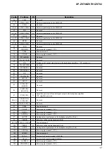


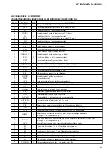
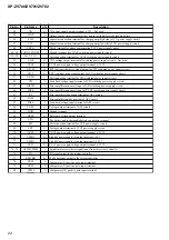


17
XP-ZV700/ZV701/ZV702
Pin No.
Pin Name
I/O
Description
56
TMS
-
Not used
57, 58
SDA8, SDA9
O
Address signal output to the SD-RAM
59
TDO
-
Not used
60, 61
SDA7, SDA6
O
Address signal output to the SD-RAM
62
TDI
-
Not used
63, 64
SDA5, SDA4
O
Address signal output to the SD-RAM
65
TEST4
-
Not used
66, 67
SDA1, SDA2
O
Address signal output to the SD-RAM
68
RTCK
-
Not used
69, 70
SDA0, SDA3
O
Address signal output to the SD-RAM
71
TCK
-
Not used
72
VDIOSD3
-
Power supply terminal (+2.7V)
73
VSS4
-
Ground terminal
74
VDIO1
-
Power supply terminal (+2.1V)
75
PI7/AIFBCK
-
Not used
76
PI6/AIFLRCK
-
Not used
77
PI5
O
Muting on/off control signal output to the headphone amplifier "H": muting on
78
PI4/AIFPCMD
-
Not used
79
PI3/XBCKO
-
Not used
80
PI2/LRCKO
-
Not used
81
PI1
-
Not used
82
PI0/PCMDO
-
Not used
83
ADCLK
-
Not used
84
DOUT
-
Not used
85
PJ7/MON7
(MONCK)
-
Not used
86
PJ6/MON6
(MONDO)
-
Not used
87
PJ5/MON5
O
Amplifier power on/off control signal output to the headphone amplifier
"H": amplifier power on
88 to 91
PJ4/MON4 to
PJ1/MON1
-
Not used
92
XRST_PWR_O
-
Not used
93
VSS6
-
Ground terminal
94
VDIO2
-
Power supply terminal (+2.1V)
95
DVDD1
-
Power supply terminal (+1.3V)
96
AVDDA1
-
Power supply terminal (+2.7V)
97
AOUTR
O
Analog audio signal output to the headphone amplifier (R-ch)
98
VREFR
O
Reference voltage output terminal (R-ch)
99, 100
AVSDA1, AVSDA0
-
Ground terminal
101
VREFL
O
Reference voltage output terminal (L-ch)
102
AOUTL
O
Analog audio signal output to the headphone amplifier (L-ch)
103
AVDDA0
-
Power supply terminal (+2.7V)
104
AVSMO
-
Ground terminal
105
EXTAL
O
System clock output terminal (22 MHz)
106
XTAL
I
System clock input terminal (22 MHz)
107
AVDMO
-
Power supply terminal (+2.7V)
108
VDIOFS256
-
Power supply terminal (+2.1V)