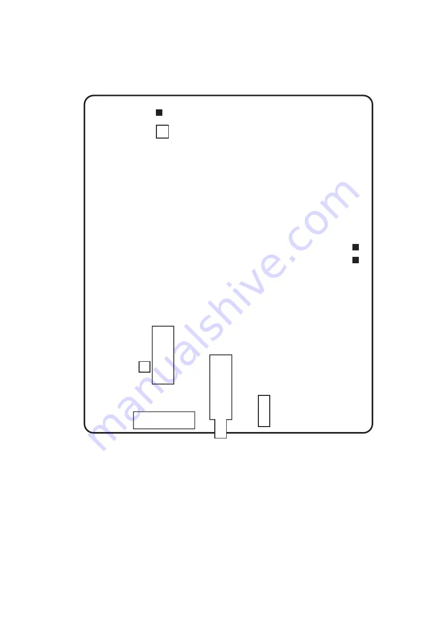
D2-5
ELECTRICAL ADJUSTMENTS
TU601
3. ELECTRICAL ADJUSTMENT PARTS LOCATION GUIDE
(VCR SECTION)
TP4002
TP4001
CP603
J4501
SYSCON PCB
IC601
L608
TP1001
C1003
Page 1: ...m sec PAL SP 5 hours max with E 300 tape LP 10 hours max with E 300 tape NTSC playback SP only 3 hours 30 minutes max with T 210 tape 1 0Vp p 75 ohm unbalanced 1 0Vp p 75 ohm unbalanced 53dB nominal S...
Page 2: ...ICON OPERATION T TEXT PRINTED CIRCUIT BOARDS OPERATION DECK OPERATION SCHEMATIC DIAGRAM DECK SCHEMATIC DIAGRAM PRINTED CIRCUIT BOARDS SYSCON Y C AUDIO HEAD AMP SCHEMATIC DIAGRAM MICON SCHEMATIC DIAGRA...
Page 3: ...a tube or tape for safety or which are assembled in the condition that these do not contact with the printed board The inside wiring is designed not to get closer to the pyrogenic parts and high volta...
Page 4: ...ck the support 2 Remove the TV VCR Block in the direction of arrow Fig 1 3 1 4 MAIN PCB Refer to Fig 1 4 1 2 3 4 5 6 Remove the screw 1 Remove the Main PCB Holder Remove the 2 screws 2 Remove the 3 sc...
Page 5: ...o Fig 1 5 1 2 3 4 5 6 Remove the 2 screws 1 Remove the 4 screws 2 Remove the screw 3 Remove the Deck Shield Plate in the direction of arrow A Remove the screw 4 Remove the Shield Plate Bottom in the d...
Page 6: ...3 B 2 4 CASSETTE HOLDER ASS Y Refer to Fig 2 4 Move the Cassette Holder Ass y to the front side Push the Locker R to remove the Cassette Side R Remove the Cassette Side L 1 2 3 Main Chassis Main Chass...
Page 7: ...Tension Adjust Unlock the 2 supports 3 and remove the Tension Band Ass y Unlock the support 4 and remove the Tension Holder 1 2 3 4 5 6 7 Tension Holder 4 2 Tension Adjust Tension Band Ass y Tension A...
Page 8: ...C HEAD Refer to Fig 2 13 A Remove the screw 1 Remove the A C Head Base Remove the 3 screws 2 Remove the A C Head and A C Head Spring 1 2 3 4 NOTE Do not touch the A C Head Use gloves When you install...
Page 9: ...NIT ASS Y Refer to Fig 2 15 Unlock the support 1 and remove the AHC Ass y Remove the 3 screws 2 Remove the Cylinder Unit Ass y 1 2 3 When you install the Cylinder Unit Ass y tighten the screws from 1...
Page 10: ...ver Loading Arm T Ass y Loading Gear S LED Reflector Fig 2 19 A NOTE When you install the Loading Arm S Ass y Loading Arm T Ass y and Main Loading Gear align each marker Refer to Fig 2 19 B Loading Ar...
Page 11: ...p up the sides of the Rubber Cap in the direction of the arrow and remove one side of the support Refer to Fig 3 2 2 GND on the CRT Screwdriver Alligator Clip Support CRT GND on the CRT Rubber Cap CRT...
Page 12: ...op Frequency Generator Front Loading Switch Frequency Modulation Frequency Sub Carrier Forward Generator Ground High Pass Filter I K L M N O P R S H SW Hz IC IF IND INV KIL L LED LIMIT AMP LM LDM LP L...
Page 13: ...or Separation Transistor Tracking Trick Playback Test Point Unregulated Volt Voltage Controlled Oscillator Video Intermediate Frequency Vertical Pulse Voltage Display Video Playback Variable Resistor...
Page 14: ...acking to the center position NOTE Also can be adjusted by pressing the ATR button for more tan 2 seconds during PLAY VOL MIN 5 POWER ON total hours and PLAY REC total hours are displayed on the scree...
Page 15: ...d parts which the rubber touches Replace when rolling becomes abnormal Clean the Head CONFIRMATION OF USING HOURS POWER ON total hours and PLAY REC total hours can be checked on the screen Total hours...
Page 16: ...lly Clean the full erase head in the same manner Refer to the figure below Audio Control Head 2 TAPE RUNNING SYSTEM When cleaning the tape transport system use the gauze moistened with isopropyl alcoh...
Page 17: ...atisfied correct DATA has been entered turn POWER off return to STANDBY MODE to finish DATA input Enter DATA SET mode by setting VOLUME to minimum While holding down VOLUME button on front cabinet pre...
Page 18: ...ent JG153 X Value Adjustment JG022 JG024A Reel Disk Height Adjustment Used to connect the Syscon PCB and CRT PCB JG162Y JG162C JG162D Used to connect the Syscon PCB and Main PCB Used to connect the te...
Page 19: ...ith the cable JG162C and JG162D Connect the Syscon PCB to the CRT PCB with the cable JG162Y Remove the Operation PCB from the set then connect it with the Syscon PCB If necessary connect CP351 Front A...
Page 20: ...on Main PCB It s possible to get the Servicing Position without the extension Jig if you arrange the unit as shown below But L503 connection can not be done Degauss circuit will not operate Be carefu...
Page 21: ...rve the chroma signal There are two types of the new alignment tape CH 1B for NTSC and CH 2 for PAL On each tape four signals 1 4 are recorded for the times and in the order shown below The TTV MP1 fo...
Page 22: ...ack in SP mode Tentelometer Video Tape Guide Roller P1 Post Fig 1 3 CONFIRMATION AND ADJUSTMENT OF REEL DISK HEIGHT 1 1 1 2 3 4 Turn on the power and set to the STOP mode Set the master plane JG022 an...
Page 23: ...pring 2 CONFIRMATION AND ADJUSTMENT OF TAPE RUNNING MECHANISM Tape Running Mechanism is adjusted precisely at the factory Adjustment is not necessary as usual When you replace the parts of the tape ru...
Page 24: ...istortion is appeared then adjust the a Reflected picture of Stamp Mark Stamp Mark Audio Control Head P4 Post Fig 2 2 A Audio Control Head 1 3 2 Fig 2 2 B Tape Audio Control Head Fig 2 2 C 0 25 0 05mm...
Page 25: ...RTS LOCATION GUIDE 1 2 3 4 5 6 7 8 9 10 12 7 8 9 10 11 12 P4 Post T Brake Spring T Reel Ass y Idler Ass y S S Brake Spring S Reel 1 Tension Adjust 2 Tension Arm 3 Guide Roller 4 P1 Post 5 Audio Contro...
Page 26: ...ppears adjustment is completed If the above adjustments doesn t work well 5 6 7 Press the VOL DOWN button on the set and the channel button 3 on the remote control simultaneously until the indicator R...
Page 27: ...H PHASE Press the PLAY or STOP button on the remote control until the vertical line becomes fit to the notch of the shadow mask 1 H PHASE 2 H BLK 3 V SIZE 50 60 4 V POSI 50 60 5 V LIN 50 60 6 V SC 50...
Page 28: ...ANGE VARIABLE knob of the oscilloscope until the range between white 100 and 0 is set to 4 scales on the screen of the oscilloscope Press the PLAY or STOP button on the remote control until the red co...
Page 29: ...ONTRAST 1 2 3 4 Using the remote control set the brightness and contrast to normal position Activate the adjustment mode display of Fig 1 1 and press the channel button 4 on the remote control to sele...
Page 30: ...D2 5 ELECTRICAL ADJUSTMENTS TU601 3 ELECTRICAL ADJUSTMENT PARTS LOCATION GUIDE VCR SECTION TP4002 TP4001 CP603 J4501 SYSCON PCB IC601 L608 TP1001 C1003...
Page 31: ...D2 6 ELECTRICAL ADJUSTMENTS TV SECTION MAIN PCB FB401 FOCUS VOLUME SCREEN VOLUME VR502 CRT PCB TP801 TP401 T501 J801...
Page 32: ...erforming adjustments in section 4 1 1 2 3 4 5 Receive the green raster pattern from color bar generator Adjust the pair of purity magnets to center the color on the screen Adjust the pair of purity m...
Page 33: ...tage of C507 is it normal No Yes Yes No Investigate R501 and F501 Whether there is output for IC501 3rd pin or not Investigate IC506 and IC501 Investigate T501 No No No No No Yes Yes Yes Yes Whether i...
Page 34: ...0MHz OSC for IC1006 67th pin and 68th pin or not Investigate X1001 Is there 135V in the emitter of Q503 Is the 5V for IC602 48th pin or not Investigate Q1006 and Q1019 Investigate IC602 Is there a hea...
Page 35: ...to IC701 1st pin or not Investigate IC701 peripheral circui Does a signal change at a volume upgrade knock down or not Is the voltage of IC352 1st pin DC 8 3V or not Investigate ICP505 D505 and D509...
Page 36: ...14th pin normal or not Yes Yes Investigate X604 No Whether is wave form of IC851 3rd pin normal or not Yes Investigate Q804 Q805 Q806 and a peripheral circuit Whether is wave form of IC602 10th pin 1...
Page 37: ...5V line Whether is a luminance signal early in IC602 34th pin or not Investigate IC602 Yes No Whether is a luminance signal early in IC4001 52th pin or not Investigate IC4001 Yes Yes R G B signal out...
Page 38: ...e wave form of the 21st pin and the 22nd pin of IC1006 is investigated Q1014 and also Q1015 are investigated The wave form of the 10th pin 11th pin and 12th pin of IC602 normal Investigate the circuit...
Page 39: ...nsert a cassette and push PLAY button No Yes No Yes Does Playback change to Stop about 6 seconds later Check IC1006 Check TAPE LOADING CAPSTAN DD UNIT and CYLINDER UNIT Check REEL SENSOR and CAPSTAN B...
Page 40: ...gnal at pin 78 or 79 of IC4001 Yes No No Is there VIDEO signal at pin 52 of IC4001 Check IC4001 and the connection of the CYLINDER Check C4035 W905 and the peripheral circuit Is there CHROMA signal at...
Page 41: ...es Check R4040 Q4006 and peripheral circuit No Yes No Is there voltage at pin 61 of IC4001 Yes Check TV Block Check IC4001 Does CHROMA signal appear at pin 52 of IC4001 Does CHROMA signal appear at pi...
Page 42: ...o Yes Yes No No Yes Replace IC4001 Check pin 52 of IC4001 and peripheral circuit Is there CHROMA signal at pin 55 of IC4001 200mVp p Replace CYLINDER UNIT Is VIDEO waveform at pin 52 of IC4001 1Vp p a...
Page 43: ...HOOTING GUIDE E 11 NO COLOR DURING SELF RECORDING AND PLAYBACK Yes No Check J4501 J701 and VIDEO input circuit Does VCR signal appear at pin 31 or 30 or 28 of IC4001 Refer to section NO COLOR DURING P...
Page 44: ...No No Yes Does Audio signal appear at pin 51 of IC601 NO NORMAL AUDIO IN PLAYBACK MODE Does Audio appear at pin 11 of IC4001 Check L4001 Q4007 and peripheral circuit Check AUDIO HEAD for debris of sta...
Page 45: ...8 of CP1004 5V No No Yes In playback is the voltage at pin 4 of CP1004 2 5V In playback check the voltage at pin 3 of CP1004 is 2V or at pin 38 of IC1006 is normal In playback is the voltage at pin 5...
Page 46: ...peripheral circuit No Yes Check POWER BLOCK Yes No Is there AUDIO signal at pins 7 or 8 or 9 of IC4001 AUDIO CAN NOT BE RECORDED Is there BIAS at pin 4 of IC4001 Check the circuit of 21 PIN and TUNER...
Page 47: ...E 15 CASSETTE IN AND DOWN BUT UNIT HAS NO FUNCTIONS No Yes Does mode indicator appear in Display Check LOADING MOTOR and the peripheral parts Does VCR operate with the remote control Yes No Check IC1...
Page 48: ...DEO input jack to IC4001 and from Tuner Pack to IC4001 Yes No Does FM signal appear at pin 2 or 4 of CP4001 Does video signal appear at pin 28 or 30 or 31 of IC4001 Does FM signal appear at pin 86 or...
Page 49: ...E E 17 NO E E NO VIDEO AND AUDIO FROM TUNER Yes No Yes Check Power PCB Is the voltage at pin 7 of TU601 5V Yes No Check IC601 Is the voltage at pin 9 of TU601 30V No Is there waveform at pins 4 and 5...
Page 50: ...voltage at pin 2 of CP1005 about DC12V Check IC1006 Check P CON 12V line and POWER BLOCK Yes No No Yes In playback is the voltage at pin 5 of CP1005 about DC1 2V CYLINDER NOT ROTATING DURING PLAYBACK...
Page 51: ...AUDIO HEAD scratched Replace AUDIO HEAD Replace CAPSTAN DD MOTOR Check peripheral components of IC1006 No Yes Yes No No Yes Does pin 8 of IC1006 output a 3 0Vp p square wave In playback is the voltage...
Page 52: ...LOADING BLOCK activate Check WORM GEAR of CASSETTE LOADING BLOCK Check EOT BOT PHOTO SENSOR pins 17 and 18 of IC1006 When a cassette is inserted is the voltage between pins 3 and 4 of CP1006 Replace L...
Page 53: ...e EOT PHOTO TRANSISTORS Check R1026 circuit Does this same problem appear when using another cassette tape When inserting a cassette does Emitter of EOT return to LOW Defective CASSETTE or CASSETTE LO...
Page 54: ...No Check pin 72 of IC1006 lines Replace IC1006 No Yes Check pin 7 of CP1004 and peripheal circuit When the FF REW is pushed does the PULSE appear at pin 72 of IC1006 Is the voltage change at pin 7 of...
Page 55: ...Yes Check Power circuit Replace CYLINDER UNIT No No Yes Yes Replace IC1006 Yes No Check REEL SENSOR Does TP4001 feed HEAD SWITCHING PULSE signal 30Hz Is the voltage at pin 2 of CP1005 UNREG 12V Does P...
Page 56: ...oise appear in the picture No No Yes By adjusting the manual tracking UP DOWN buttons will the noise disappear in the picture Check P B ENVELOPE No Yes Are GUIDE POSTS the right height Adjust GUIDE PO...
Page 57: ...ONTALLY AUTO TRACKING DOES NOT OPERATE By manual tracking does the DC level at pin 19 of IC1006 change Yes No In auto tracking is the voltage at pin 19 of IC1006 more than DC0 7V Yes No Replace IC1006...
Page 58: ...MOTOR rotate Refer to section CAPSTAN DD MOTOR NOT ROTATING Is CAPSTAN BELT normal Yes No Replace CAPSTAN BELT Yes No Does REEL SENSOR PULSE signal appear at pin 32 of IC1006 Check Reel Sensor of Q100...
Page 59: ...IC1006 Yes No Replace CYLINDER MOTOR Replace CYLINDER MOTOR Does pin 108 of IC1006 output a 5Vp p square wave In playback is the voltage at pin 5 of CP1005 about 1 2V PLAYBACK PICTURE SHAKES Is FG Pu...
Page 60: ...Auto setup 22 ANB MESECAM H IN Input terminal of MESECAM or NOT 23 AVSS AVSS Ground 24 P50 FF REW L OUT Not used 25 P51 LDM_RVS OUT Output signal to control the rotation direction of the loading motor...
Page 61: ...AT 5 V 64 X2 X2 OUT Subclock pluse 32 768KHz 65 X1 X1 IN Subclock pluse 32 768KHz 66 RES RES IN RESET will be done when the voltage goes to HIGH after the restart signal 67 OSC1 OSC1 IN Connect the m...
Page 62: ...utput terminal control for T REC LED voltage drive 97 P87 REC LED OUT Output terminal control for REC LED voltage drive 98 C SYNC C SYNC IN Input terminal for composite C SYNC 99 AUDIO FF Hi Fi_H SW O...
Page 63: ...SERVO TIMING CHART IC1006 OEC0078C F2 1 CH 2 CH 1 REC CTL REC 6 PIN V SYNC TRICK PB 110 PIN DPG 107 PIN DFG 108 PIN H SW P 100 PIN WAVEFORM CHANGES DEPENDED ON THE TAPE SPEED V SYNC E E 98 PIN...
Page 64: ...CLUTCH DIRECT CONNECTION PINCH ROLLER LOADING DIRECTION FWD CAPSTAN FWD ROTATING DIRECTION CAPSTAN RVS ROTATING DIRECTION LIGHT RECEIVING LIGHT RECEIVING H LIGHT GUARD LIGHT RECEIVING LIGHT GUARD LIGH...
Page 65: ...0 G23 RMPG06J G3 MTZJ6 8B T 77 GP15M G23 RU2AM V1 RB721QT 77 RD12FB T7 SB10 03A3 RU2YX V1 IC 16PIN 20PIN 100PIN 8PIN 24PIN 3PIN TC74HC4053AP ET317 HA118217F S 24C08ADPA 01 LC74772V RE5VS31A 28PIN 112P...
Page 66: ...733 C T P Q 2SC1740SP TP 2SC2412KT146 R S 2SB892 S T AE DTC114TSTP DTC114EKT147 2SC1815Y TPE2 2SC2271 D E AE 2SC2274 AA 2SC2909 S T AA 2SC3000 AA 2SC945 C T P Q 2SD734 E F AA GP1S94L 2SD2599 DTA114EKA...
Page 67: ...XT_G TEXT_Y VD AFT_M 12 11 BUS MICON OPERATION 49 48 6 1 4 3 L608 3 PUMP UP THERMAL PROTECTION 2 SYNC T TEXT 4 13 ABL MICON OPERATION PLL P2C Q607 CUT OFF TEXT_Y Q806 BLUE AMP Q805 Q804 GREEN AMP RED...
Page 68: ...006 BUFFER 88 87 89 86 H AMP 8 7 REC MUTE LINE MUTE ENV DET J4501 2 1 6 3 8 7 11 16 15 20 19 Q4507 PERI SW Q4509 AMP Q4505 MUTE SW L4001 TRAP Q4007 AMP Q4501 Q4502 BUFFER D4510 D4511 L4005 1 3 6 Q4004...
Page 69: ...G OUT B OUT R OUT TV Q1014 TV POWER SW TV_POWER_H 85 VCR_MUTE VCR_A_MUTE 100 VIDEO H SW H SW 83 TUNER_MUTE TU_AUDIO_MUTE_H 60 REMOCON 3 2 1 OS753 AT 5V D793 D791 D792 P CON 5V_B POWER ON SW Q4201 21 T...
Page 70: ...053AP 5 RSTB OSC1 5 6 OSC2 X851 13875KHz 12 TCLK 19 SYNC 17 WIND SSIG 2 1 TSIG 3 CSIG Q855 RED BUFFER Q852 GREEN BUFFER Q851 BLUE BUFFER Q862 BLK BUFFER 1 2 3 4 5 12 11 10 Y C_VIDEO 21_G 21_B 21_R 21_...
Page 71: ...C781 R773 R774 C779 R772 C751 R793 R762 R780 R777 R776 R759 R760 R766 C752 R763 R754 R761 R350 C351 W807 W818 W808 W002 W003 R351 B702 B701 W812 C353 C354 W004 C702 W811 C356 C355 CD351_2 C755 CD750_2...
Page 72: ...J2630 010070 1 2 3 4 5 6 7 OF PRINTING AND SUBJECT TO CHANGE WITHOUT NOTICE NOTE THIS SCHEMATIC DIAGRAM IS THE LATEST AT THE TIME DESCRIBED IN PARTS LIST ONLY CRITICAL FOR SAFETY USE ONES ARE SINCE TH...
Page 73: ...MARKED BY CAUTION DURING PLAYBACK MEASURED WITH THE DIGITAL TESTER NOTE THE DC VOLTAGE AT EACH PART WAS OF PRINTING AND SUBJECT TO CHANGE WITHOUT NOTICE NOTE THIS SCHEMATIC DIAGRAM IS THE LATEST AT T...
Page 74: ...R4043 R4045 C4087 IC4002 R4046 R4047 C4090 Q4003 R4013 R4012 C657 R864 R868 Q863 R863 R1078 R1084 R1081 R1062 C1053 R1063 C1044_1 Q1015 Q1016 C1055 R1013 R1059 C1035 C1038 R1032 Q4509 C643 R655 R4201...
Page 75: ...134 W076 W075 W080 W068 W099 W090 W261 R623_1 C4064 W113 W118 L4016 W086 W088 W030 W029 W028 W252 W867 Q1011 R1036 W166 W170 R615 W167 W173 W168 D4002 W054 W144 W211 W111 W829 W830 C667 X601 X4001 W03...
Page 76: ...19 C620 C651 C652 L609 C4518 C4506 L601 D4501 C4504 L4501 W195 W053 R1083 R1050 R1079 R1019 W072 C1040 D858 D860 R1016 W007 W008 D854 IC1099 C1021 C1003 D1002 W016 C862_1 C867_1 L851 L852 C856_1 IC852...
Page 77: ...793 JM VPS PDC IC 1 10 11 12 13 14 15 16 17 18 19 2 20 21 22 23 24 3 4 5 6 7 8 9 CAUTION DIGITAL TRANSISTOR TP4001 H SW TP4002 V ENV S801X S801Y S809Y S804X S812X S820X S820Y S821Y S821X AUDIO SIGNAL...
Page 78: ...R NOTE THE DC VOLTAGE AT EACH PART WAS D1005 RD12FB D1008 MTZJ5 6B Q352 DTA124EKA MAIN POWER OFF MUTE SW IC1003 LC74772V OSD IC 1 10 11 12 13 14 15 16 17 18 19 2 20 21 22 23 24 3 4 5 6 7 8 9 CAUTION D...
Page 79: ...K1 4W R658 100 1 4W R624 1K R622 680K R636 1K R661 330 R680 1 5K R656 10K 1 4W R646 100K R653 100 R648 100 R669 1K R638 120K R641 1K 1 4W R673 220 1 4W R674 2201 4W C642 3 3 50V KA C652 1 50V KA C635...
Page 80: ...SC2412K W885 W843 W860 W907 W867 W857 W818 W859 W892 W919 W863 W855 W931 W900 W927 Q4502 2SA1037AK BUFFER L4502 100uH L4501 100uH DURING PLAYBACK MEASURED WITH THE DIGITAL TESTER NOTE THE DC VOLTAGE A...
Page 81: ...812 Q1019 2SB892 P CON 5V DRIVER DURING PLAYBACK MEASURED WITH THE DIGITAL TESTER NOTE THE DC VOLTAGE AT EACH PART WAS Q1010 DTA114EKA DRIVER CAUTION DIGITAL TRANSISTOR CAP_VCO AT 12V P CON 5V MOTOR_G...
Page 82: ...AL FOR SAFETY USE ONES ARE SINCE THESE PARTS MARKED BY CAUTION OF PRINTING AND SUBJECT TO CHANGE WITHOUT NOTICE NOTE THIS SCHEMATIC DIAGRAM IS THE LATEST AT THE TIME CP302_1 B2B EH A 1 2 C361 0 001 B...
Page 83: ...1 1K R878 6 8K R856 1K R879 1K R919 10K R876 100 1 4W R877 100 1 4W R881 1K R882 1K C857 100 16V YK C854 470 6 3V YK C852_1 220 6 3V KA C882 3 3 50V KA C883 3 3 50V KA C881 3 3 50V KA C872 100 16V KA...
Page 84: ...2 W015 CP401 Q502 W031 C423 R503 R506 D518 RY501 R553 Q503 CP803A HS503 HS501 W010 W045 Q805 R801 C801 J 8 0 1 CP801 T P 8 0 2 R 8 0 5 R815 R812 W041 Q804 C820 R808 T P 8 0 1 R 80 2 T P 8 0 3 R 8 1 0...
Page 85: ...432 0 47 100V TF C450 120P 2KV BP C430_1 0 001 500V B C409 0 0022 M C416 22P 500V SL C417 560P 500V B C418_1 1 160V MHE C421_1 1000 35V MHE OF PRINTING AND SUBJECT TO CHANGE WITHOUT NOTICE NOTE THIS S...
Page 86: ...3 IC505 KIA7806PI 6V POWER REG IC 1 2 3 IC502 NJM7805FD 5V REG IC 1 2 3 CAUTION DIGITAL TRANSISTOR IC501 STR F6707 POWER REG IC 1 2 3 4 5 HS503 763WAE0108 HS502 763WAA0046 HS505 763WAA0046 HS501 763W...
Page 87: ...AND SUBJECT TO CHANGE WITHOUT NOTICE NOTE THIS SCHEMATIC DIAGRAM IS THE LATEST AT THE TIME DESCRIBED IN PARTS LIST ONLY CRITICAL FOR SAFETY USE ONES ARE SINCE THESE PARTS MARKED BY CAUTION DANS LA NO...
Page 88: ...CON 9V MOTOR GND AUDIO OUT J801 CRT SOCKET 10 4 3 1 7 5 6 9 8 VIDEO IN GND GND GND R G B SW RED GND NC NC GND GREEN GND AUDIO IN AUDIO IN BLUE GND GND PERI CTL TUNER VIDEO OUT TUNER AUDIO OUT TUNER AU...
Page 89: ...number in the schematic diagram NOTE WAVEFORMS 1 5V 0 1ms div 7 20V 20 s div TV POWER 3 0 5V 10ms div 8 10V 10ms div TV POWER DEFLECTION CRT DEFLECTION J 1 11 PB 2V 10ms div Y C AUDIO HEAD AMP 12 PB 1...
Page 90: ...iv 20 REC 10V 5 s div MICON 21 POWER ON 1V 50ns div 18 POWER ON 50mV 1ms div 22 POWER ON 1V 20 s div 23 POWER ON 2V 20 s div 24 POWER ON 2V 5ms div 25 PB 50mV 10ms div 26 PB 50mV 0 5ms div WAVEFORMS 2...
Page 91: ...ms div CHROMA IF 34 POWER ON 5mV 1ms div 35 POWER ON 0 5V 20 s div 36 POWER ON 0 5V 20 s div 37 POWER ON 0 5V 20 s div 38 POWER ON 0 5V 10ms div 39 POWER ON 200mV 50 s div 40 POWER ON 2V 50 s div 41 P...
Page 92: ...2 221 218 110 214 114 113 205 108 221 112 107 136 A 112 221 215 115 217 110 206 201 129 203 203 201 138 130 130 142 143 142 143 140 141 128 145 123 116 208 208 118 127 B 147 148 SP351 208 PCB030 OPERA...
Page 93: ...MECHANICAL EXPLODED VIEW K1 2 A 133 206 206 207 134 212 PCB010 SYSCON PCB 202 210 202 122 J4501 103 106 209 121 137 TU601 204 204 204 B 135 131 220 111 216 144 144 216 102 105 220...
Page 94: ...S1 072 308 040 UT2 3 8 1 208 S1 106 30A 040 UIT 3 10 22 120 S1 3WP A01 100 GUIDE REMOCON 1 209 S1 102 30A 020 VT2 3 10 2 121 SHIELD COVER 1 122 SHILED CASE 1 210 87 741 095 410 SCREW TAP TITE P FLAT 3...
Page 95: ...or each position NOTE KYODO OIL SLIDAS No 150 BA OIL 505 UN4001 334 321 348 507 H5001 506 305 304 501 356 301 347 316 317 313 508 315 338 512 310 361 329 359 368 357 366 351 364 308 306 366 358 365 35...
Page 96: ...346 312 331 514 344 512 330 AA AA AA AA AA AD AA AA AA AA AA AA AA BA AC AA AD AD PART NO CLASS MARK GREASE G 555G AA G 488M AB MG 33 AD FL 721 AC NOTE Applying positions AA AB AC AD and BA for the gr...
Page 97: ...1 511 S2 P26 600 5N0 PW CUT 2 6 6 0 5 3 323 S5 OA9 002 130 LINK ASS Y 1 512 S2 Q26 471 3N0 PW 2 6 4 7 0 13 3 324 S5 OA9 002 160 LINK LEVER ASS Y 1 513 S2 P18 450 5N0 PW CUT 1 8 4 5 0 5 1 325 S5 OP2 00...
Page 98: ...0 CAP E 100 6 3V D852 87 020 465 010 DIODE 1SS133T C693 87 010 112 080 CAP E 100 16V D854 S3 Z68 V10 000 ZENER MTZJ6 8B C852 87 015 975 080 CAP E 220 6 3V D855 87 020 465 010 DIODE 1SS133T C854 87 010...
Page 99: ...35_0_9985_0 Q1001 8Z JU1 603 010 PHOTO COUPLER GP1S566 Q1002 89 324 122 080 TR 2SC2412KT SWITCH Q1003 S0 02G 004 900 PHOTO COUPLER GP1S94L Q1005 8Z JU1 603 010 PHOTO COUPLER GP1S566 SW1001 S5 082 210...
Page 100: ...VBED010 C537 87 015 694 080 CAP E 0 47 50V SW795 S5 042 01T 310 SW TACT SKHVBED010 C538 S5 EZT 147 1M0 CAP E 470 10V SW796 S5 042 01T 310 SW TACT SKHVBED010 C540 S5 EZT B10 0M0 CAP E 10 160V SW797 S5...
Page 101: ...IVE 305Y002S SW501 S5 302 050 010 SW PLUS SDDFC3056A T501 S4 813 504 0W0 TRANS SWITCHING 8135040W CONNECTOR VARIABLE RESISTOR CP504 S6 973 200 390 CORD UX CONNECTOR VR502 S1 263 L2B TC0 SFR RH063MCN2R...
Page 102: ...2 11 IKENOHATA 1 CHOME TAITO KU TOKYO 110 JAPAN TEL 03 3827 3111 737004 Printed in Singapore...