background image

– 24 –

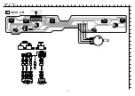
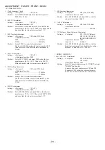
ADJUSTMENT  <TUNER / FRONT / DECK>

< TUNER  SECTION >

1. Clock Frequency Check

Settings : • Test point :

TP2 (CLK)

Method : Set to MW 1602 kHz and check that the test point is

2052 kHz ± 45 Hz.

2. MW VT Adjustment

Settings : • Test point :

TP1 (VT)

• Adjustment location : L953

Method : Set to MW 1710 kHz and adjust L953 so that the test

point becomes 8.0 V ± 0.05 V. Then set to MW 530 kHz

and check that the test point is more than 0.3 V.

3. MW Tracking Adjustment

Settings : • Test point :

TP8 (Lch), TP9 (Rch)

• Adjustment location :

L952 ................................................... 603 kHz

TC941 ............................................... 1404 kHz

Method : Set up TC941 to center before adjustment.

The level at 630 kHz is adjusted to maximum by L952.

Then the level at 1404 kHz is adjust to maximum by

TC941.

4. SW VT Adjustment

Settings : • Test point :

TP1 (VT)

• Adjustment location : L942

Method : Set to SW 17.9 MHz and adjust L942 so that the test

point becomes 8.0 V ± 0.05 V. Then set to SW 5.73

MHz and check that the test point is more than 0.3 V.

5. SW Tracking Adjustment

Settings : • Test point :

TP8 (Lch), TP9 (Rch)

• Adjustment location :

L941 .................................................5.73 MHz

TC943 ...............................................17.9 MHz

Method : Set up TC943 to center before adjustment.

The level at 5.73 MHz is adjust to maximum by L941.

Then the level at 17.9 MHz is adjust to maximum by

TC943.

6. FM VT Adjustment

Settings : • Test point :

TP1 (VT)

• Adjustment location : L906

Method : Set to FM 108.0 MHz and adjust L906 so that the test

point becomes 7.0 V ± 0.1 V. Then set to FM 87.5 MHz

and check that the test point is more than 0.5 V.

7. FM Tracking Adjustment

Settings : • Test point :

TP8 (Lch), TP9 (Rch)

• Adjustment location: L903

Method : Set to FM 98.0 MHz and adjust L903 so that the

test point is less than 9 dBµV.

8. AM  IF Adjustment

Settings : • Test point :

TP8 (Lch), TP9 (Rch)

• Adjustment location :

L802 ................................................... 450 kHz

9. DC  Balance / Mono Distortion Adjustment

Settings : • Test point :

TP3, TP4 (DC Balance)

TP8 (LCH), TP9 (RCH)

(MONO DISTORTION)

• Adjustment location : L801

• Input level :

60 dBµV

Method : Set to FM 98.0 MHz and adjust L801 so that the

distortion is minimun. Next, check that the voltage

between TP3 and TP4 is 0 V ± 500 mV.

< FRONT  SECTION >

10. µ-CON  OSC  Adjustment

Settings : • Test point :

TP5 (KEY-SCAN)

TP6 (GND)

• Adjustment location : L501

Method : Insert  AC  plug  while  pressing  of  "TUNER"  key  and

"POWER" function key.

Connect a frequency counter across TP5 and TP6.

Then adjust L501 so that the test point becomes

92.470 Hz ± 0.092 Hz (92.378 Hz ~ 92.562 Hz).

Summary of Contents for NSX-VC220

Page 1: ... BASIC TAPE MECHANISM ZZM 3 PR2NM BASIC CD MECHANISM BZG 2 MVSD3NM NSX VC220 HR S M Code No 09 01A 449 8R1 This Service Manual is the Revision Publishing and replaces Simple Manual of NSX VC220 HR S M Code No 09 018 449 8T1 If requiring information about the CD mechanism see Service Manual of BZG 2 S M Code No 09 00C 353 2N6 REVISION ...

Page 2: ...s 2 channels stereo Frequency response 50 Hz 8 kHz Recording system AC bias Heads DECK 1 playback x 1 DECK 2 recording playback x 1 erase x 1 DISC PLAYER Laser Semiconductor laser λ 780 nm D A converter 1 bit dual Signal to noise ratio 90 dB 1 kHz 0 dB Harmonic distortion 0 05 1 kHz 0 dB Video signal NTSC PAL color system selectable Video data MPEG 1 Audio data MPEG 1 Layer 2 VCD MPEG 1 Layer 3 MP...

Page 3: ...tsättas för osynling laserstrålning som överskrider gränsen för laserklass 1 PROTECTION OF EYES FROM LASER BEAM DURING SERVICING CAUTION Use of controls or adjustments or performance of proce dures other than those specified herin may result in hazardous radiation exposure ATTENTION L utillisation de commandes réglages ou procédures autres que ceux spécifiés peut entraîner une dangereuse expositio...

Page 4: ...in power 2 2 2 2 2 Confirm that the main power is turned on and the HOLD terminal of the MICROCOMPUTER keeps the H level or not 3 3 3 3 3 When the HOLD terminal is L level the abnormality detection circuit is judged to be working correctly and the MICROCOMPUTER is judged to be good 1 Forced discharge of electrolytic capacitor of power supply block When repair is going to be attempted in the set th...

Page 5: ... ends of the electrolytic capacitor C113 that is connected to VDD of the MICROCOMPUTER with tweezers 3 3 3 3 3 Connect the AC power cord again If the MICROCOMPUTER returns to the normal operation the MICROCOMPUTER is good Note The reference number or MICROCOMPUTER pin number of transistor Q110 and electrolytic capacitor C113 can change depending on the models Be sure to check the reference numbers...

Page 6: ...Z F C125 87 010 759 080 C CAP U 0 1 25F C126 87 010 759 080 C CAP U 0 1 25F C127 87 010 759 080 C CAP U 0 1 25F C128 87 010 759 080 C CAP U 0 1 25F C131 87 012 286 080 CAP U 0 01 25 C132 87 012 286 080 CAP U 0 01 25 C133 87 A12 368 080 C CAP S 0 1 50 Z F C166 87 010 759 080 C CAP U 0 1 25 Z F C181 87 A12 074 080 CAP E 470 25 M C401 87 A12 319 080 C CAP U 0 1 25 K B C402 87 A12 319 080 C CAP U 0 1 ...

Page 7: ...0 400 040 CAP E 0 47 50 C508 87 012 172 080 CAPACITOR CHIP U 10P CH C509 87 012 198 080 C CAP U 180P 50 J SL C510 87 A10 039 080 CAP U 470P 50 C511 87 010 759 080 C CAP U 0 1 25F C512 87 012 336 080 C CAP U 330P 50 B C513 87 010 829 080 CAP U 0 047 16 C514 87 012 286 080 CAP U 0 01 25 C515 87 012 274 080 CHIP CAP U 1000P 50B C516 87 010 759 080 C CAP U 0 1 25F C517 87 010 176 080 C CAP U 680P 50 B...

Page 8: ...964 87 010 175 080 C CAP S 560P 50 J SL C971 87 A12 067 080 CAP ELECT 330 16V C972 87 A12 090 080 CAP ELECT 4 7 50V C973 87 012 286 080 C CAP U 0 01 25 K B C974 87 012 286 080 C CAP U 0 01 25 K B C979 87 012 195 080 C CAP U 100P 50 J CH C981 87 A12 071 080 CAP ELECT 47 25V C982 87 010 759 080 C CAP U 0 1 25F C983 87 012 286 080 C CAP U 0 01 25 K B C984 87 012 286 080 C CAP U 0 01 25 K B C987 87 01...

Page 9: ...57 080 RES M F 0 15 1W J R132 87 A00 257 080 RES M F 0 15 1W J TH101 87 A91 042 080 C THMS 100K 55001 TH102 87 A91 042 080 C THMS 100K 55001 DECK C B CN1 87 099 753 010 CONN 11P H 9604 CNA401 86 ZM3 604 210 CONN ASSY 3P PB CNA451 8B NFA 626 010 CONN ASSY 8P RPB SFR1 87 024 581 010 SFR 3 3K H KVSF637A SOL1 82 ZM3 627 010 SOL ASSY 27SO SOL2 82 ZM3 627 010 SOL ASSY 27SO SW1 87 036 109 010 SW MICRO SP...

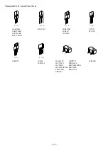
Page 10: ...585BC CSC4115BC KTC3198GR B C E 2SK360E B C E D S G B C E 2SA1981Y E C B 2SB1370E 2SB1677 2SD2619 CC5551 STC250 G D S 2SK2937 E C B 2SJ460 2SK2541 2SA1235F 2SC2714O 2SC3052F 2SC5345SF S O CSD1306E SBT5401 SBT5551 KRA102S KRC102S RTK KRC104S KRA107S ...

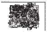
Page 11: ... 11 WIRING 1 MAIN FRONT TUNER 32 31 30 29 28 27 26 25 24 23 22 21 20 19 18 17 16 15 14 13 12 11 10 9 8 7 6 5 4 3 2 1 A B C D E F G H I J K L M N O P Q R S T U ...

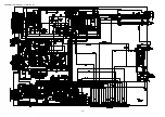
Page 12: ... 12 SCHEMATIC DIAGRAM 1 MAIN 1 2 ...

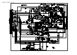
Page 13: ... 13 SCHEMATIC DIAGRAM 2 FRONT DECK ...

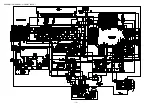
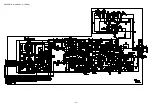
Page 14: ... 14 SCHEMATIC DIAGRAM 3 TUNER ...

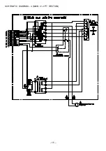
Page 15: ... 15 SCHEMATIC DIAGRAM 4 MAIN 2 2 PT SECTION ...

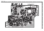
Page 16: ... 16 WIRING 2 AMP 32 31 30 29 28 27 26 25 24 23 22 21 20 19 18 17 16 15 14 13 12 11 10 9 8 7 6 5 4 3 2 1 A B C D E F G H I J K L M N O P Q R S T U ...

Page 17: ... 17 SCHEMATIC DIAGRAM 5 AMP ...

Page 18: ... 13 12 11 10 9 8 7 6 5 4 3 2 1 18 A B C D E F G H I J K L M N O P Q R S T U WIRING 3 DECK SW5 CAM2 SW1 CAM1 SOL1 SOL2 SW2 CST1 SW3 REA SW4 CST2 IC2 1 3 IC1 1 3 L H R1 SFR1 TO FRONT C B CN504 FFC504 CN1 1 3 5 7 9 11 2 4 6 8 10 W1 M1 TAPE MOTOR L H E DECK C B ...

Page 19: ... 19 IC BLOCK DIAGRAM ...

Page 20: ... 20 FL HNA 10SS19T GRID ASSIGNMENT ANODE PIN CONNECTION GRID ASSIGNMENT ANODE CONNECTION PIN CONNECTON ...

Page 21: ... CD IC acknowledge input 24 CD CE O CD DATA VCD O CD enable output CD data output 25 I TUNE IFC I Tuner SD detection input Tuner IF count input 26 I RDS DATA I O Tuner RDS data input Connected to GND through a resistor O STB ECHO VCD Strobe output for shift register 27 I WRQ I CD DATA I CD WRQ input CD data input VCD 28 I RDS CLK I O Tuner RDS clock input DSP data output Connected to GND through a...

Page 22: ... REA I DECK 2 side A recordable switch data input L REC 61 CAM1 I DECK 1 CAM STOP switch data input 62 AUTO2 I DECK 2 AUTO STOP switch data input 63 AUTO1 I DECK 1 AUTO STOP switch data input 64 CAM2 I DECK 2 CAM switch data input 65 REB I DECK 2 side B recordable switch data input L REC 66 CST2 I DECK 2 cassette detect switch data input 67 P1 I AM 10K I O FL segment P1 output AM10K data input Not...

Page 23: ... 23 Pin No Pin Name I O Description 81 90 P13 P22 O FL segment P13 P22 output 91 100 G1 G10 O FL grid G1 G10 output ...

Page 24: ...to center before adjustment The level at 5 73 MHz is adjust to maximum by L941 Then the level at 17 9 MHz is adjust to maximum by TC943 6 FM VT Adjustment Settings Test point TP1 VT Adjustment location L906 Method Set to FM 108 0 MHz and adjust L906 so that the test point becomes 7 0 V 0 1 V Then set to FM 87 5 MHz and check that the test point is more than 0 5 V 7 FM Tracking Adjustment Settings ...

Page 25: ...z signal with respect to that of the 315 Hz signal is 0 dB 3 dB 14 PB Sensitivity Check DECK 1 DECK 2 Settings Test tape TTA 200 Test point TP8 Lch TP9 Rch Method Play back the test tape and check that the output level of the test point is 110 mV 3 dB 15 REC PB Frequency Response Check DECK 2 Settings Test tape TTA 602 Test point TP8 Lch TP9 Rch Input signal 8 kHz 1 kHz 20 VU 0dB Method Apply a 1 ...

Page 26: ...ration STOP button Play button PAUSE button FF button RWD button REC REC MUTE button Display All indicators light READING Normal Normal CD TEST CD TEST All indicators light Function All FL indicators light LD illuminates all the time Focus search continuous operations 1 Spindle motor continuous kick Normal playback If TOC cannot be read focus search is continued Tracking servo OFF ON Each time PAU...

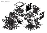
Page 27: ...a PWB PWB PWB HT SINK FL BZG 2 CABI BOTTOM PLATE SHIELD 1 2 3 4 5 6 7 8 9 10 11 12 13 14 15 16 17 40 18 38 19 41 20 8 11 12 21 CUSH 11 8 5 2 23 28 26 27 28 29 30 31 33 34 35 36 37 39 24 25 25 32 22 PLATE EARTH MIC A A A A A A WIRE BINDER WIRE BINDER WIRE BINDER WIRE ASSY 160 BLK 24 WIRE ASSY LUG WIRE ASSY 160 BLK 24 ...

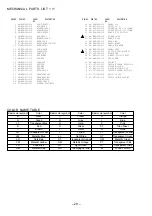
Page 28: ... 224 010 SPR C LOCK 12 82 NF5 229 010 PLATE LOCK 13 8B NHA 002 010 CABI FR H 14 8B NFA 015 110 KEY POWER 15 8B NFA 017 010 KEY FUN 16 8B NFA 011 010 RING OPE 17 8B NFA 018 010 KEY OPE 18 8B NFA 016 010 KEY GEQ 19 8B NFA 020 010 KEY REC 20 87 NF4 217 110 HLDR LOCK 2 21 8A NFA 011 110 KNOB RTRY VOL 22 8B NFA 013 110 KNOB RTRY MIC 23 8B NFA 222 010 HLDR HT SINK 24 8B NHA 003 010 PANEL TRAY H 25 87 A9...

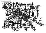
Page 29: ... 9 10 11 10 11 12 12 13 13 14 14 15 15 16 16 18 18 19 19 20 20 21 21 30 22 23 24 25 26 27 28 22 23 24 25 26 27 28 29 31 32 33 34 35 36 37 37 38 38 39 39 40 41 42 43 44 51 52 45 46 47 48 49 50 53 54 54 17 55 30 35 29 31 32 33 52 51 44 45 43 42 IC EW732 IC EW732 b a a b c c 40 41 46 47 48 49 PWB ...

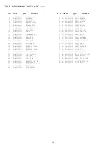
Page 30: ...25 8Z ZM3 226 010 SPR C FR M3 26 8Z ZM3 250 010 GEAR SLIP F R A M3 27 8Z ZM1 269 010 FELT FF REW 2 28 8Z ZM1 238 110 GEAR SLIP FF REW B 2 29 8Z ZM3 220 010 LEVER FR M3 30 8Z ZM3 205 010 LEVER PLAY M3 31 8Z ZM3 233 010 SPR T BRG M3 32 84 ZM2 227 310 SPR C AZIMUTH 33 87 A90 403 110 HEAD RPH MS15R 34 87 A90 404 010 HEAD EH LE15B 35 8Z ZM3 239 010 SPR E FR 36 8Z ZM3 211 010 LEVER EJECT R 37 8Z ZM3 225...

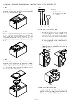
Page 31: ...stall it turning to clockwise direction until click sound comes out Remove the grill frame and four pieces of rubber caps by pulling out with a flat bladed screwdriver Remove the screws from hole where installed rubber caps Insert a flat bladed screwdriver into the position indicated by the arrows and remove the panel Re move the screws of each speaker unit and then remove the speaker units TOOLS ...

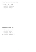
Page 32: ...AMIC 4 8B NSL 019 010 SPKR CERAMIC ASSY 5 8B NSL 610 010 SPKR 120 20 2 ACCESSORIES PACKAGE LIST DESCRIPTION REF NO KANRI NO PART NO 1 8B NHA 901 010 IB H ECA M 2 87 043 115 010 FEEDER ANT FM 3 87 006 226 010 ANT LOOP AM 4 87 A90 119 010 ANT WIRE SW 5M 5 8B NHK 702 010 RC UNIT RC BAS09 VS 6 87 A92 262 010 PLUG CONVERSION WT01011 7 87 A80 167 010 CORD PIN 1PY 150CM ...

Page 33: ...2 11 IKENOHATA 1 CHOME TAITO KU TOKYO 110 JAPAN TEL 03 3827 3111 Printed in Singapore 9301978 9720501 921338 ...

Reviews: