– 42 –
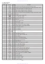
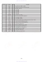
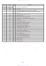
39
RVSS
–
Right channel one-bit DAC R channel ground. (Must be connected to 0V)
40
RCHO
O
Right channel one-bit DAC R channel output.
41
RVDD
–
Right channel one-bit DAC R channel power supply.
42
MUTER
O
Right channel one-bit DAC R channel mute ouput. (Not connected)
43
XVDD
–
Crystal oscillator power supply.
44
XOUT
O
Connection for a 16.934MHz crystal oscillator element.
45
XIN
I
46
XVSS
–
Crystal oscillator ground. (Must be connected to 0V)
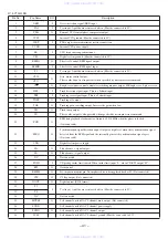
47
SBSY
O
Subcode block synchronization signal output. (Not connected)
48
EFLG
O
C1, C2 single and double error correction monitor pin. (Must be connected to 0V)
49
PW
O
Subcode P, Q, R, S, T, U, V and W output. (Not connected)
50
SFSY
O
Subcode frame synchronization signal output. This signal falls when the subcode are in the
standby state. (Not connected)
51
SBCK
I
Subcode readout clock input. This is a Schmitt input. (Must be connected to 0V)
52
FSX
O
Output for the 7.35 kHz synchronization signal divided from the crystal oscillator.
(Not connected)
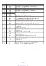
53
WRQ
O
Subcode Q output standby output.
54
RWC
I
Read/write control input. This is a Schmitt input.
55
SQOUT
O
Subcode Q output.
56
COIN
I
Command input from the control microprocessor.
57
CQCK
I
Command input read clock or subcode readout input clock from SQOUT pin.
This is a Schmit input
58
RES
I
Reset pin. This pin must be set low briefly after power is first applied.
59
T11
O
Test output. Leave open. (Normally outputs a low level). (Not connected)
60
16M
O
16.9344 MHz output. (Not connected)
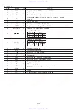
61
4.2M
O
4.2336 MHz output.
62
T5
I
Test input. A pull-down resistor is built in. (Must be connected to 0V)
63
CS
I
Chip select input. A pull-down resistor is built in. (Must be connected to 0V)
I
Test input. No pull-down resistor. (Must be connected to 0V)
Pin No.
Pin Name
I/O
Description
www. xiaoyu163. com
QQ 376315150
9
9
2
8
9
4
2
9
8
TEL 13942296513
9
9
2
8
9
4
2
9
8
0
5
1
5
1
3
6
7
3
Q
Q
TEL 13942296513 QQ 376315150 892498299
TEL 13942296513 QQ 376315150 892498299

