background image

– 33 –

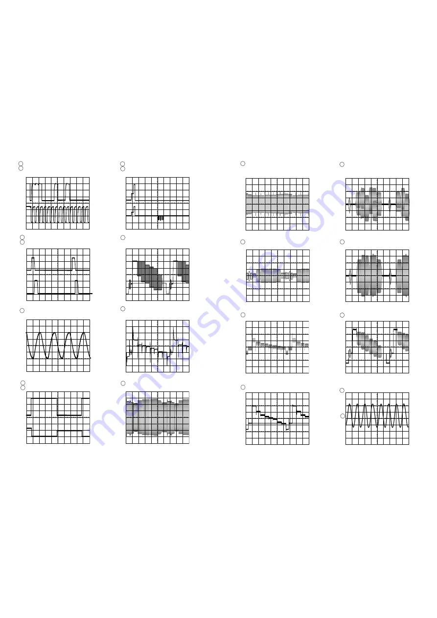
WAVEFORM
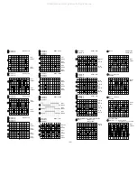
<VIDEO SECTION>

    IC301 PIN 10 (SDA-R)

           MODE: REC

    IC301 PIN 11 (SCL-R)

2V/div
20

µ

S/div

IC401 PIN 16 (HD)

MODE: REC

IC401 PIN 01 (C-SYNC)

2V/div
10

µ

S/div

Q301 Emitter (FSC)

MODE: REC

50mV/div
0.1

µ

S/div

IC301 PIN 41 (C-ROT)

MODE: REC

CN301 PIN 3 (HSW-V)

2V/div
5mS/div


IC401 PIN 14 (JOG VD

MODE: PB

     IC401 PIN 14 (BLANK)

2V/div
1mS/div


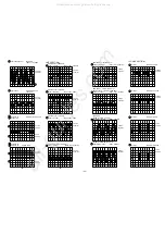
IC301 PIN 55 (V IN)

MODE: REC

200mV/div
10

µ

s/div

     IC301 PIN 57 (WDC)

MODE: REC

200mV/div
10

µ

s/div

     Q307 Emitter (REC YC)

MODE: REC

100mV/div
10

µ

s/div

            NORM

SMS

C

2V

       2V

 A=20

µ

s

            NORM

SMS

C

2V

       2V

 A=10

µ

s

50mV

                 A=0.1

µ

s

            NORM

SMS

C

2V

       2V

 A=5ms

            NORM

SMS

C

2V

       2V

 A=1ms

A3       0.0  %

        LINES

200m~


 10

µ

s

          v

A3       0.0  %

        LINES

200m~


 10

µ

s

          v

A3       0.0  %

        LINES

100m~


 10

µ

s

          v

IC301 PIN 63 (PB YFM)

MODE: PB

200mV/div
10

µ

S/div

IC301 PIN 64 (PB CSL)

MODE: PB

50mV/div
10

µ

S/div

IC301 (DE EMPH)

MODE: PB

200mV/div
10

µ

S/div

IC301 PIN 42 (Y CCD OUT)

MODE: PB

200mV/div
10

µ

S/div

A3       0.0  %

        LINES

200m~


 10

µ

s

          v

A3       0.0  %

        LINES

  50m~


 10

µ

s

          v

A3       0.0  %

        LINES

200m~


 10

µ

s

          v

A3       0.0  %

        LINES

200m~


 10

µ

s

          v

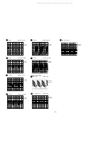
IC301 PIN 24 (C CCD OUT)

MODE: PB

100mV/div
10

µ

S/div

IC301 PIN 13 (PB C)

MODE: PB

100mV/div
10

µ

S/div

Q309 Emitter (V OUT)

MODE: PB

200mV/div
10

µ

S/div

<SYSTEM SECTION>

IC101 PIN 74

1V/div
50nS/div

A3       0.0  %

        LINES

100m~


 10

µ

s

          v

A3       0.0  %

        LINES

100m~


 10

µ

s

          v

A3       0.0  %

        LINES

200m~


 10

µ

s

          v

2

1

3

4

8

9

10

5

11

13

12

6

7

14

17

18

15

19

16

20

20

All manuals and user guides at all-guides.com

Summary of Contents for HV-FX8700

Page 1: ...BASIC VIDEO MECHANISM NC3600 P4LRH HV FX8700 K EH S M Code No 09 008 437 3N1 If requiring information about the mechanism see Service Manual of NCP4LHR3600 S MCode No 09 995 333 1n1 All manuals and u...

Page 2: ...layback only SP 33 35 mm sec LP 16 67 mm sec EP 11 12 mm sec Rewind time Approx 1 min with E 180 tape Channel coverage VHF Low EH E2 4 S1 6 VHF High EH E5 12 S7 41 UHF 21 69 RF output UHF channel betw...

Page 3: ...3 All manuals and user guides at all guides com...

Page 4: ...C B to mechanism that the marked position of the rotary switch on the MAIN C B must agree with the corresponding marking on the MAIN C B See the above illustration MAIN C B Mechanism The washers that...

Page 5: ...50 7L C112 87 010 197 080 C CAP S 0 01 0 25 KB C113 87 010 197 080 C CAP S 0 01 0 25 KB C114 87 010 197 080 C CAP S 0 01 0 25 KB C115 87 010 197 080 C CAP S 0 01 0 25 KB C116 87 015 681 080 CAP E 10 1...

Page 6: ...7 010 313 080 C CAP S 18P 50 C369 87 010 196 080 C CAPACITOR S 0 1 25 C371 87 012 156 080 C CAP S 220P 50 CH C374 87 010 196 080 C CAPACITOR S 0 1 25 C375 87 010 196 080 C CAPACITOR S 0 1 25 C376 87 0...

Page 7: ...LR50 L552 87 005 432 080 COIL 10UH K FLR50 L553 87 005 432 080 COIL 10UH K FLR50 M101 8Z JU1 609 010 STATOR DMNVS PS101 8Z JU1 603 010 SNSR GP15566 PS102 8Z JU1 603 010 SNSR GP15566 R90 87 029 115 010...

Page 8: ...0 C CAP S 56P 50 J CH C931 87 010 178 080 C CAP S 1000P 50 K B C2012 C933 87 010 405 080 CAP E 10 50 M ML SME C934 87 010 180 080 C CAP S 1500P 50 K B C2012 C935 87 012 140 080 C CAP S 470P 50 J CH C9...

Page 9: ...E BEAD BL02RN2 FC1 87 033 213 080 CLAMP FUSE PFC500 FC2 87 033 213 080 CLAMP FUSE PFC500 ICF2 87 A91 337 080 PROTECTOR IC ICP N75 ICF3 87 001 211 080 PROTECTOR IC ICP N50 ICF4 87 001 132 080 PROTECTOR...

Page 10: ...E C B 2SA933AS 2SC1741AS 2SA1037 2SC2412K DTA114EK DTC114EK DTC143TK 2SB1436 B C E 2SB1237 2SB1443 2SD1858TV2 E C B 2SC3708ST DTC144EK KRA104S KRC102S E C B E C B PT493F B C E C E All manuals and use...

Page 11: ...11 FL 10 MT 113G GRID ASSIGNMENT ANODE CONNECTION GRID ASSIGNMENT ANODE CONNECTION All manuals and user guides at all guides com a l l g u i d e s c o m...

Page 12: ...12 C WIRE HARNESS DIAGRAM All manuals and user guides at all guides com...
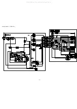
Page 13: ...BLOCK DIAGRAM 1 SYSCON SERVO 13 All manuals and user guides at all guides com...
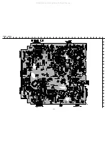
Page 14: ...BLOCK DIAGRAM 2 VIDEO 14 All manuals and user guides at all guides com...
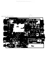
Page 15: ...BLOCK DIAGRAM 3 HIFI THEATRE 15 NOT USE WIDE WIDE All manuals and user guides at all guides com...
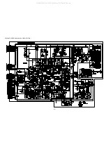
Page 16: ...16 BLOCK DIAGRAM 4 TUNER All manuals and user guides at all guides com a l l g u i d e s c o m...

Page 17: ...17 BLOCK DIAGRAM 5 MPX All manuals and user guides at all guides com...
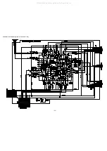
Page 18: ...BLOCK DIAGRAM 6 CANAL 18 SWITCH Q610 WIDE All manuals and user guides at all guides com...
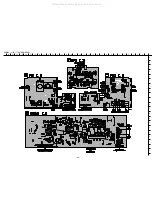
Page 19: ...19 BLOCK DIAGRAM 7 POWER PS All manuals and user guides at all guides com...
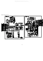
Page 20: ...32 31 30 29 28 27 26 25 24 23 22 21 20 19 18 17 16 15 14 13 12 11 10 9 8 7 6 5 4 3 2 1 A B C D E F G H I J K L M N O P Q R S T U WIRING 1 MAIN 20 All manuals and user guides at all guides com...
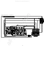
Page 21: ...21 SCHEMATIC DIAGRAM 1 MAIN 1 4 SYSTEM SECTION All manuals and user guides at all guides com a l l g u i d e s c o m...

Page 22: ...22 SCHEMATIC DIAGRAM 2 MAIN 2 4 VIDEO SECTION All manuals and user guides at all guides com...
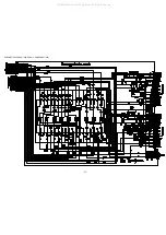
Page 23: ...23 SCHEMATIC DIAGRAM 3 MAIN 3 4 HIFI SECTION All manuals and user guides at all guides com...
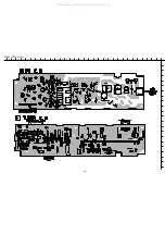
Page 24: ...31 30 29 28 27 26 25 24 23 22 21 20 19 18 17 16 15 14 13 12 11 10 9 8 7 6 5 4 3 2 1 A B C D E F G H I J K L M N O P Q R S T U WIRING 2 FR1 FR2 MPX REAR 24 All manuals and user guides at all guides co...

Page 25: ...25 SCHEMATIC DIAGRAM 4 FR1 FR2 All manuals and user guides at all guides com...
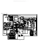
Page 26: ...26 SCHEMATIC DIAGRAM 5 REAR 1 2 THEATRE SECTION All manuals and user guides at all guides com a l l g u i d e s c o m...

Page 27: ...27 SCHEMATIC DIAGRAM 6 REAR 2 2 CANAL SECTION All manuals and user guides at all guides com...
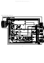
Page 28: ...32 31 30 29 28 27 26 25 24 23 22 21 20 19 18 17 16 15 14 13 12 11 10 9 8 7 6 5 4 3 2 1 A B C D E F G H I J K L M N O P Q R S T U WIRING 3 TUNER PS 28 All manuals and user guides at all guides com...
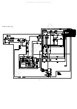
Page 29: ...29 SCHEMATIC DIAGRAM 7 TUNER All manuals and user guides at all guides com...
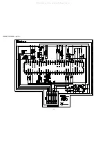
Page 30: ...30 SCHEMATIC DIAGRAM 8 MAIN 4 4 POWER SECTION All manuals and user guides at all guides com...

Page 31: ...31 SCHEMATIC DIAGRAM 9 PS All manuals and user guides at all guides com a l l g u i d e s c o m...

Page 32: ...32 SCHEMATIC DIAGRAM 10 MPX All manuals and user guides at all guides com...

Page 33: ...NORM SMSC 2V 2V A 1ms A3 0 0 LINES 200m 10 s v A3 0 0 LINES 200m 10 s v A3 0 0 LINES 100m 10 s v IC301 PIN 63 PB YFM MODE PB 200mV div 10 S div IC301 PIN 64 PB CSL MODE PB 50mV div 10 S div IC301 DE E...

Page 34: ...IC101 PIN 33 2V div 10 S div 2V div 10 S div IC106 PIN 7 MODE P1 PB IC106 PIN 8 IC106 PIN 9 IC101 PIN 39 5V div 5mS div 5V div 5mS div 5V div 5mS div 5V div 5mS div CN103 PIN 9 MODE P1 SLOW CN103 PIN...

Page 35: ...N 32 IC101 PIN 41 5 div 5mS div 5V div 5mS div 5V div 5mS div 5V div 5mS div CN103 PIN 4 MODE P1 PB IC104 PIN 27 50mV div AC 1mS div 5V div 1mS div IC101 PIN 39 MODE P1 PB IC104 PIN 4 IC104 PIN 15 5V...

Page 36: ...Hz 27kHz div 0 5V div 0 2 S div POWER SECTION IC1 PIN 3 MODE Power ON 200V div 5 S div IC1 PIN 3 MODE Power SAVE 200V div 5 S div IC1 PIN 2 MODE Power ON 2V div 5 S div IC1 PIN 2 MODE Power SAVE 2V di...

Page 37: ...s 2V 5 s 10V 5 s 10V 5 s PT1 PIN 14 MODE Power ON 10V div 5 S div PT1 PIN 14 MODE Power SAVE 10V div 5 S div TUNER SECTION C812 TU V CHECK LAND 0 2V div 20 S div Q811 Collector TU V CHECK LAND 0 5V d...

Page 38: ...38 IC BLOCK DIAGRAM All manuals and user guides at all guides com...
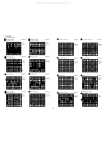
Page 39: ...nts Of Errors State 0 NORMAL 1 DRUM ERROR WHEN DRUM FG DOES NOT CHANGE OVER 2SEC 2 T REEL ERROR WHEN T REEL DOES NOT CHANGE OVER 6SEC 3 S REEL ERROR WHEN S REEL DOES NOT CHANGE OVER 6SEC 4 LOADING UNL...

Page 40: ...center Short TR RST CN301 5 to GND CN301 2 An indication appears on the FL display tube indicating that the machine is in the adjustment mode 2 Press A TR key in the remote controller to activate HSW...

Page 41: ...LEVEL I Video envelope detection input for audio tracking Analog input 61 AFT I AFT voltage read out A D input 62 AGC I AGC voltage read out A D input Description Pin No Pin Name I O IC DESCRIPTION IC...

Page 42: ...etection input 2 11 12 NC Not use 3 SPDATA O Serial data signal 4 7 IN4 1 I Shuttle switch signal input 4 1 8 GND GND 9 STRB I TC4021 chip select signal 10 CLK I Serial clock signal 13 14 IN5 6 I Jog...

Page 43: ...5 0 5 0 76 5 0 5 0 5 0 77 2 1 2 1 2 0 78 2 7 2 6 2 6 79 0 0 2 0 80 0 0 2 0 81 0 2 0 2 0 82 4 5 4 5 4 6 83 0 0 0 84 0 0 0 PIN NO EE REC PB 85 5 1 5 1 5 0 86 0 0 0 87 4 8 4 8 4 8 88 5 0 5 0 5 0 89 5 0 5...

Page 44: ...PB E 15 3 15 1 15 1 C 13 7 12 9 12 9 B 15 3 15 1 15 1 Q109 2SB1443 PIN EE REC PB E 0 0 0 C 26 3 25 9 25 9 B 0 0 0 Q107 KRC104S PIN EE REC PB E 26 4 25 9 25 9 C 13 1 12 1 12 2 B 26 3 25 9 25 9 Q102 2SB...

Page 45: ...2 0 0 0 3 5 1 5 1 5 1 IC701 NJL68H380 PIN EE REC PB E 0 0 0 C 4 4 4 4 4 4 B 0 0 0 Q701 2SD1858 PIN EE REC PB E 0 0 0 C 4 4 4 4 4 4 B 0 0 0 Q702 2SC2412KR PIN EE REC PB E 0 0 0 C 3 8 3 8 3 8 B 0 0 0 Q...

Page 46: ...F G G G 17 D D PWB D 11 A 10 9 8 PWB PWB I B CABI MAIN 21 C SHLD PLATE PIN JACK SHLD PLATE MPXB SHLD PLATE PS SHLD PLATE MPXB SHLD PLATE BTTM SHLD PLATE JG PWB PWB PWB PWB C B I 5 1 2 3 4 B B MECHANI...

Page 47: ...STAY 6 8Z JU2 015 010 KEY REC 2 7 8A JU1 001 010 CABI FR 8 8A JU1 018 010 PLATE BBE 9 87 B00 002 010 BADGE AIWA 30 ABS SIL 10 8Z JU1 016 010 WINDOW LED 11 8Z JU2 014 010 KEY DEMO 2 12 8A JU1 010 010...

Page 48: ...2 11 IKENOHATA 1 CHOME TAITO KU TOKYO 110 JAPAN TEL 03 3827 3111 Printed in Singapore 912204 0251431 All manuals and user guides at all guides com...
Reviews: