


32
O
O
O
—
O
I
I
I
O
—
I
O
—
I
I
I
I
I
I
I
I
O
O
—
O
I
I
I
O
O
O
O
O
O
O
O
O
—
—
O
O
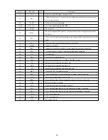
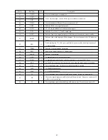
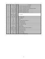
CD read/write control output.
Data output to sound processor IC (M62495FP).
Clock output to sound processor IC (M62495FP).
Not Connected.
Clock shift output of the microcomputer.
Hold status detection.
Microcomputer reset.
Connected to 32.768kHz crystal oscillator.
GND.
Connected to 5.76MHz Ceramic Filter.
Power supply for microcomputer (+5V).
FM STEREO status input.
KEY AD input.
CD DOOR SW status detection input.
KEY AD input.
DECK MECHA MOTOR status input.
REC status input.
FM, AM status input. (Not connected)
Data input from tuner PLL.
BASS LED ON/OFF control output. (Not connected)
Q-Sound LED ON/OFF control output.
Not connected.
INT DIODE MATRIX detection output.
CD RF level detection input.
CD sub-code Q standby input.
Remote control input.
LCD segment output and initial settings output. (SW) (Not connected)
LCD segment output and initial settings output. (LW) (Not connected)
LCD segment output and initial settings output. (MW 10K)
LCD segment output and initial settings output. (FM WIDE) (Not connected)
LCD segment output and initial settings output. (OIRT) (Not connected)
LCD segment output and initial settings output. (SW2) (Not connected)
LCD segment output and initial settings output. (SYN)
LCD segment output and initial settings output.
Power supply for microcomputer (+5V).
GND.
LCD segment output.
LCD segment output. (Not Connected)
O-RMC/CE
O-DATA
O-CLK
NC
O-CLK SFT
I-HOLD
I-RST
XT1 (IN)
XT2 (OUT)
VSS1
CF1 (IN)
CF2 (OUT)
VDD1
I-FM ST
I-KEYO
I-CD SW
I-KEY1
I-MOTOR
I-REC
I-FM/AM (NC)
I-TU DO
O-BASS LED (NC)
O-QS LED
NC
O-INT
I-DRF
I-WRQ
I-REMO
SO/PAO (NC)
S1/PA1 (NC)
S2/PA2
S3/PA3 (NC)
S4/PA4 (NC)
S5/PA5 (NC)
S6/PA6
S7/PA7
S8-S11
VDD3
VSS3
S12-S19
S20-S23 (NC)
1
2
3
4
5
6
7
8
9
10
11
12
13
14
15
16
17
18
19
20
21
22
23
24
25
26
27
28
29
30
31
32
33
34
35
36
37-40
41
42
43-50
51-54
IC, LC867132V-5P07
Pin No.
Pin Name
I/O
Description
Summary of Contents for CSD-EL300 EZ(S)
Page 8: ...8 LCD DISPLAY LCD AIW4213...
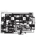
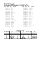
Page 9: ...10 9 SCHEMATIC DIAGRAM 1 MAIN...
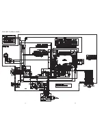
Page 10: ...12 11 SCHEMATIC DIAGRAM 2 CD MAIN...
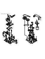
Page 11: ...1 2 3 4 5 6 7 8 9 10 11 12 13 14 A B C D E F G H I J K 14 13 WIRING 1 MAIN CD MAIN...
Page 14: ...20 19 SCHEMATIC DIAGRAM 4 FRONT SOL2...
Page 15: ...1 2 3 4 5 6 7 8 9 10 11 12 13 14 A B C D E F G H I J K 22 21 WIRING 4 FRONT...
Page 17: ...25 IC BLOCK DIAGRAM IC TA2149N IC LC72121M...
Page 19: ...27 IC LA6541D...
Page 34: ...2 11 IKENOHATA 1 CHOME TAITO KU TOKYO 110 JAPAN TEL 03 3827 3111 737004 Printed in Singapore...