1
2
3
4
5
6
7
8
9
10
11
12
13
14
A
B
C
D
E
F
G
H
I
J
K
WIRING-1 (MAIN/CD)
R318
R317
R8200
R8190
C317
All manuals and user guides at all-guides.com
Page 1: ...A11T3C COMPACT DISC STEREO CASSETTE RECEIVER CSD A100 S M Code No 09 003 342 2R6 G S V S R E V I S I O N This Service Manual is the Revision Publishing and replaces Simple Manual S M Code No 09 003 34...
Page 2: ...04 010 IB G E FM GSC 1 8A CDA 907 010 IB V ER FM VSC 2 87 050 076 010 AC CORD SET ASSY E VSC 2 87 A80 144 010 AC CORD SET ASSY G BLK GSC Design and specifications are subject to change without notice...
Page 3: ...osition aux radiations ADVARSEL Usynlig laserst ling ved bning n r sikkerhedsafbrydereer ude af funktion Undg uds ttelse for str ling This Compact Disc player is classified as a CLASS 1 LASER product...
Page 4: ...080 CAP ELECT 1 50V C829 87 010 178 080 CHIP CAP 1000P C830 87 010 178 080 CHIP CAP 1000P C833 87 018 195 080 CAP CER 1200P 16V C834 87 010 248 080 CAP ELECT 220 10V C843 87 010 197 080 CAP CHIP 0 01...
Page 5: ...6P CD ME L401 87 003 102 080 COIL 10UH L404 87 003 152 080 COIL 100UH R840 87 029 124 010 RES FUSE 2 2 1 4 SFR430 87 024 437 080 SFR100K RH063EC X401 8Z CD5 633 010 VIB CER16 93MHZ FCR16 93M2 FRONT C...
Page 6: ...EX ACD GSC L5 87 A50 649 010 COIL FM2 OSC V ACD VSC L6 87 A50 337 010 COIL AM OSC TOKO VSC L7 87 A50 579 010 COIL AM IFT ACD L8 87 A50 335 010 COIL FM IFT TOKO L9 87 A50 577 010 COIL FM DET ACD L10 87...
Page 7: ...e Value of resistor Chip resistor Wattage Type Tolerance 1 16W 1 10W 1 8W 1608 2125 3216 5 5 5 CJ CJ CJ Form L W t 1 6 0 8 0 45 2 1 25 0 45 3 2 1 6 108 118 128 A A CHIP RESISTOR PART CODE 0 55 Resisto...
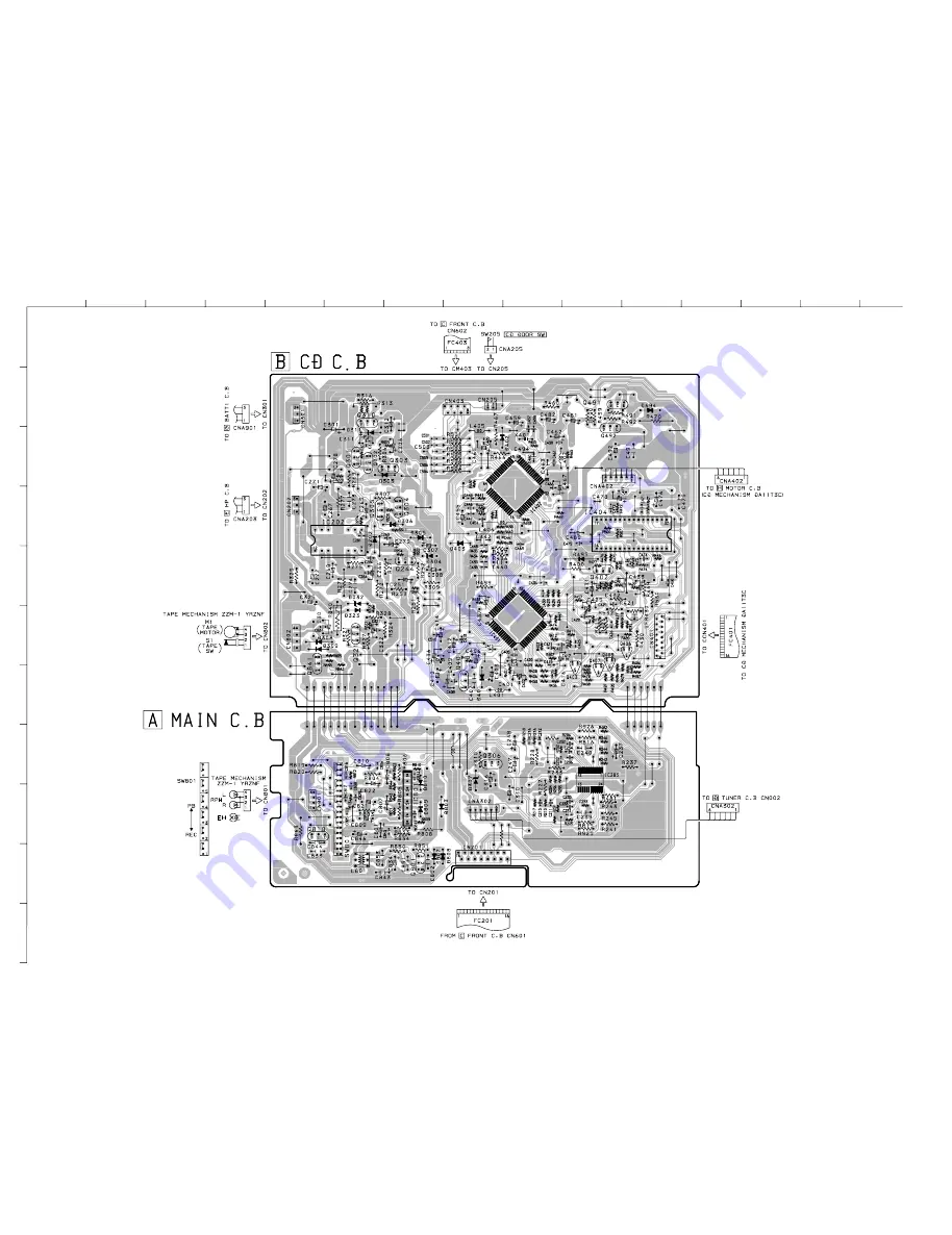
Page 8: ...1 2 3 4 5 6 7 8 9 10 11 12 13 14 A B C D E F G H I J K 10 9 WIRING 1 MAIN CD R318 R317 R8200 R8190 C317 All manuals and user guides at all guides com...
Page 9: ...S133 C484 220P C483 220P 270 270 R236 3 9k R217 JR R218 JR 2 2k R838 JR R311 JR R312 JR C280 JR C281 JR R822 22k R821 22k R820 8 2k R819 8 2k 1 4W R808 220 1 4W IC801 NJM14558LD TO DECK CHASSIS JW129...
Page 10: ...14 13 SCHEMATIC DIAGRAM 2 CD All manuals and user guides at all guides com...
Page 11: ...E LIMIT SW M2 SLED MOTOR TO B CD C B CNA402 H MOTOR C B _ 16 15 TRANSISTOR ILLUSTRATION E B C E C B E C B E C B BCE 2SC2714 DTC114TK DTC114YK DTC124XK DTC144TK 2SA1296 2SC1815 2SA933 2SC1740 DTC114TS...
Page 12: ...1 2 3 4 5 6 7 8 9 10 11 12 13 14 A B C D E F G H I J K 18 17 WIRING 3 FRONT HP BATT1 BATT2 JW604 AC230V 50Hz C627 C628 C629 C630 C631 All manuals and user guides at all guides com...
Page 13: ...NM JW604 4 7k 6224 NM NM 6224 NM NM NM NM NM NM NM NM JW605 1 H JW606 1 H C630 100 10V C629 0 01 JW603 FB C631 0 01 DTC114TK JR604 4 7k JR605 4 7k JW615 1k JW614 1k JW613 1k C627 0 01 JW608 1 H JW633...
Page 14: ...1 2 3 4 5 6 7 A B C D E F G H I J K WIRING 4 TUNER VSC 22 21 1 2 3 4 5 6 7 A B C D E F G H I J K WIRING 5 TUNER GSC C038 All manuals and user guides at all guides com...
Page 15: ...24 23 SCHEMATIC DIAGRAM 4 TUNER VSC SCHEMATIC DIAGRAM 5 TUMER GSC FM BALANCE ADJ 470 FM BPF JW FM RFEX L005 FM OSC EX CH C038 0 01 HVC202A All manuals and user guides at all guides com...
Page 16: ...8 FM IF Adjustment Settings Test point IC001 LA1828 19PIN Adjustment location L008 Method Adjust L008 so that the output level at 98 0MHz becomes balanced 9 FM Balance Adjustment Settings Test point I...
Page 17: ...ency 10 7MHz 0 1MHz Stereo separation More than 25dB at 98 0MHz AM SECTION VSC GSC Sensitivity Less than 48dB at 603kHz S N 10dB Less than 46dB at 999kHz Less than 44dB at 1404kHz Distortion Less than...
Page 18: ...ing phase compensation constants are connected between the TD and VR pins Tracking phase compensation setting pin Tracking jump signal kick pulse amplitude setting pin Tracking control signal output p...
Page 19: ...evel by the DSP Digital system GND Output pin to which external focus search smoothing capacitor is connected Tracking Balance Control EF balance variable range setting pin No connection Disc defect d...
Page 20: ...automatic selection monitoring output pin Rough servo at H Phase servo at L Track detect signal input pin Schmidt input Tracking error signal input pin Schmidt input Tracking OFF output pin Tracking...
Page 21: ...ed to 0V when not in use Pin outputting the 7 35 kHz sync signal which is generated by dividing frequency of crystal oscillator Subcode Q output standby output pin Read write control input pin Schmidt...
Page 22: ...rnal 5 76 MHz ceramic filter Microprocessor power supply 5V Key AD input AD Key AD input AD Deck status input AD CD door switch status input Main clock shift output Not connected BASS LED ON OFF contr...
Page 23: ...NC SEG DP SEG A SEG B SEG C SEG D NC O O O O O Not connected SEG DP control SEG A control SEG B control SEG C control SEG D control Not connected Pin No Pin Name I O Description All manuals and user g...
Page 24: ...A 622 010 FF CABLE 8P CD FR 21 8A CDA 016 110 KEY CD 22 87 063 165 010 OIL DMPR 150 23 8A CDA 017 110 KEY MODE 24 88 CH6 220 010 CUSHION CD A 25 8A CDA 621 010 FF CABLE 16P CD RF 26 8A CDA 012 110 CHA...
Page 25: ...3 24 25 26 27 28 29 30 31 33 34 35 36 37 38 39 40 41 42 43 44 45 46 47 48 49 50 51 8 P C B P C B P C B P C B P C B P C B DA11T3C ZZM 1 P C B 60 60 P C B 54 C C A A A A A A A A A A A A A G A A A A A A...
Page 26: ...IMUTH 24 8Z ZM1 216 010 LEVER AUTO 25 8Z ZM1 246 010 SPR T AUTO 2 26 8Z ZM1 233 010 GEAR IDL REW 27 8Z ZM1 208 010 LEVER STOP 28 8Z ZM1 207 010 LEVER FF 29 8Z ZM1 206 010 LEVER REW 30 8Z ZM1 211 110 L...
Page 27: ...P101NR REF NO PART NO KANRI DESCRIPTION NO CD MECHANISM PARTS LIST 1 1 1 S2 121 A28 400 COVER GEAR 2 S2 511 A21 000 GEAR MIDDLE 3 S2 511 A21 100 GEAR DRIVE A S1 PN2 03R OSE SCR PAN PCS 2 3 B 87 261 07...
Page 28: ...2 11 IKENOHATA 1 CHOME TAITO KU TOKYO 110 JAPAN TEL 03 3827 3111 H251701 Printed in Singapore All manuals and user guides at all guides com...