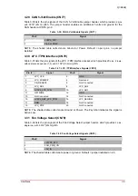
Interfaces
29
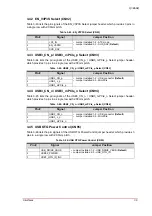
Q7-BASE
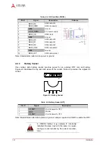
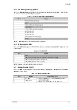
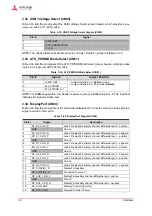
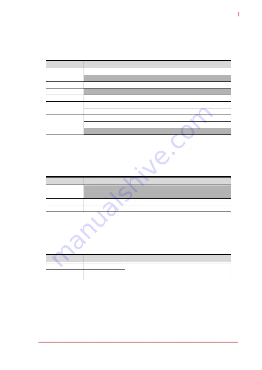
3.15 CPLD Programming (CN52)
Table 3-16 lists the pin signals of the CPLD Programming header, which provides
10 pins, 2 rows,
with odd/even sequence and 0.100
"
(2.54mm)
pitch.
NOTE: The shaded table cells denote Power or Ground.
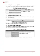
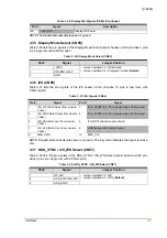
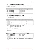
3.16 FAN Control (CN53)
Table 3-17 lists the pin signals of the CPU fan header, which provides 4 pins in a single row with
2.54mm pitch.
NOTE: Shaded table cells denote power or ground.
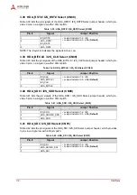
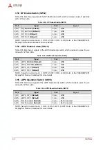
3.17 Battery Enable (CN57)
Table 3-18 lists the pin signals of the coin cell battery enable jumper header, which provides 2
pins with 2.00mm pitch.
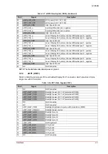
Table 3-16: CPLD Programming Signals (CN52)
Pin #
Signal
1
POST_TCK (Test Clock)
2
GND
3
POST_TDO (Test Data Output)
4
+V3P3_ATX
5
POST_TMS (Test Mode Select)
6
Not Connected
7
Not Connected
8
Not Connected
9
POST_TDI (Test Data Input)
10
GND
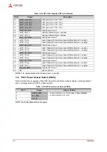
Table 3-17: FAN (CN53)
Pin #
Signal
1
GND
2
FAN_VCC (+V12P0_ATX or +V5P0A [selected by CN79])
3
FAN_TACH_IN (measures fan speed)
4
FAN_PWM_OUT (sets fan speed)
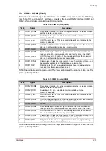
Table 3-18: Battery Enable (CN57)
Pin #
Signal
Jumper Position
1
3V_BAT
• Jumper Installed (1-2) - coin cell battery socket
enabled (
Default
)
• Empty - coin cell battery socket disabled
2
+VDD_RTC