background image

Getting Service 

Customer Satisfaction is top priority for ADLINK Technology Inc. If you need 
any help or service, please contact us at 

Ask an Expert:


http://askanexpert.adlinktech.com

. 


ADLINK Technology, Inc. 

Web Site 

http://www.adlinktech.com 

Sales & Service  [email protected] 

Telephone 

+886-2-8226-5877 

Fax 

+886-2-8226-5717 

Address 

9F, No. 166, Jian Yi Road, Chungho District, New Taipei County 
Taiwan 235 


Summary of Contents for PXI-7921

Page 1: ...PXI 7921 24 ch Multiplexer DPDT Relay Module User s Manual Manual Rev Rev 1 1 Date February 8 2020 Part Number 50 17011 1010...

Page 2: ...idental or consequential damages arising out of the use or inability to use the product or documentation even if advised of the possibility of such damages This document contains proprietary informati...

Page 3: ...mers are encouraged to dispose of them in accordance with the product disposal and or recovery programs prescribed by their nation or company Battery Labels for products with battery California Propos...

Page 4: ...elp or service please contact us at Ask an Expert http askanexpert adlinktech com ADLINK Technology Inc Web Site http www adlinktech com Sales Service Service adlinktech com Telephone 886 2 8226 5877...

Page 5: ...to a PXI Platform 6 Chapter 3 Signal Connection 9 3 1 PXI 7921 Topology 9 3 2 PXI 7921 Pin Assignments Descriptions 10 3 3 TB 6221 Terminal Board 13 2 wire MUX 14 2 wire 2 group MUX 15 2 wire 4 group...

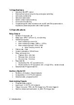
Page 6: ...INK switch modules features specifications and applications Chapter 2 Installation Describes how to install a switch module into a PXI chassis For software library and utilities installation please re...

Page 7: ...ditional field wiring For safety critical applications PXI 7921 module can switch to the preset state by either asserting emergency shutdown manually or watchdog timer overflow event 1 1 Features PXI...

Page 8: ...switching voltage 220VDC 125VAC Max switching power 50VA 60W Max carrying current 2A Failure rate 10 A Contact resistance 100m max Relay set reset time Operate time 4ms max Release time 4ms max Bounc...

Page 9: ...pin D submale Operating temperature 0 to 55 C Storage temperature 20 to70 C Humidity 5 to 95 non condensing Power requirements when all relays are activated simultaneously 5V 3 3V 1A 400mA Dimensions...

Page 10: ...4 Introduction This page intentionally left blank...

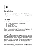
Page 11: ...ipping materials and carton for future storage or shipping 2 2 Unpacking ADLINK switch module contains sensitive electronic components that can be easily damaged by static electricity The switch modul...

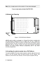
Page 12: ...front panel for wiring purposes and the J1 J2 IEC connectors in the rear are used to link the chassis backplane With its modular rugged and high shock resistant mechanical features the switch module f...

Page 13: ...llation 7 insert the switch module into the chassis Once inserted a click can be heard from the ejector latch Tighten the screws on the front panel Figure 2 Installing the switch module into a PXI pla...

Page 14: ...This page intentionally left blank 8 Installation...

Page 15: ...up of 12 1 4 wire multiplexer These configurations are totally software programmable The PXI 7921 typically connects one instrument such as a DMM or digitizer to many measurement points or a signal so...

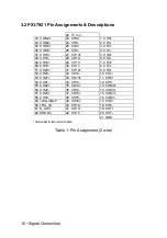
Page 16: ...H2 49 CH19 29 CH11 7 CH3 50 CH19 30 CH11 8 CH3 51 CH20 31 CH12 9 CH4 52 CH20 32 CH12 10 CH4 53 CH21 33 CH13 11 CH5 54 CH21 34 CH13 12 CH5 55 CH22 35 CH14 13 COM0 56 CH22 36 CH14 14 COM0 57 CH23 37 CH1...

Page 17: ...CH17 19 CH7 62 SHDNn 42 CH41 20 CH31 21 GND not used in one wire mode Table 2 Pin Assignment 1 wire 22 5 VOUT 43 COM2 23 CH8A 1 CH0A 44 COM2 24 CH8A 2 CH0A 45 COM3 25 CH9A 3 CH1A 46 COM3 26 CH9A 4 CH...

Page 18: ...instrument to advance the switch card to the next scan entry S_ADV Output Scanner Advanced Trigger to an instrument that indicated the switch card has advanced to the next scan and relays are debounce...

Page 19: ...consists of a printed circuit with screw terminals The terminal block connects directly to the front panel I O connector of the PXI 7921 The TB 6221 s default printed circuit is in 2 wire mode If othe...

Page 20: ...Signal Connection 2 wire MUX This configuration has one 24x1 2 wire multiplexer Bank0 which has twenty four channels The following diagram illustrates the terminal board pin definition Figure 3 24x1 M...

Page 21: ...ection 15 2 wire 2 group MUX This configuration has two 12x1 2 wire multiplexers Bank0 and Bank1 each has twelve channels The following diagram illustrates the terminal board pin definition Figure 4 T...

Page 22: ...tion 2 wire 4 group MUX This configuration has four 6x1 2 wire multiplexers Bank0 Bank1 Bank2 and Bank3 each has six channels The following diagram illustrates the terminal board pin definition Figure...

Page 23: ...nal Connection 17 1 wire MUX This configuration has one 48x1 1 wire multiplexer Bank0 which has forty eight channels The following diagram illustrates the terminal board pin definition Figure 6 48x1 M...

Page 24: ...8 Signal Connection 4 wire MUX This configuration has one 12x1 4 wire multiplexer Bank0 which has twelve channels The following diagram illustrates the terminal board pin definition Figure 6 4 wire MU...

Page 25: ...ndshaking the switch module provides eight channels of programmable digital I O interface to facilitate general purpose control applications To make full use of the flexible trigger and signaling syst...

Page 26: ...ecify one time or cyclic scanning of scanlist entries This operating mode supports trigger signals for instrument handshaking For more information on handshaking signals please refer to section 4 3 4...

Page 27: ...and ready to take a new measurement The waveform polarity and pulse width of Scanner Advanced signal can also be software programmed For more information on scanlist configuration please refer to the...

Page 28: ...the Scanner Advanced is set to pulsating mode Trigger In Scanner Advanced Relay status P Pattern 3 4 Operation start Figure 10 Handshaking operation Scanner Advanced set in pulsating mode Trigger In S...

Page 29: ...e two times to guarantee that measurement devices take measurements after the signal path is fully settled and the relays switch as close as possible to their maximum operating speed As the scan delay...

Page 30: ...ctions below to ensure the handshake functions properly 1 Configure ADLINK PXI switch module s Trigger In to rising edge triggered Scanner Advanced output in active low pulsating mode with pulse width...

Page 31: ...ng users guide 4 4 Trigger Bus PXI specification defines eight bused lines across slots in a segment Users can route various trigger signal to synchronize multiple PXI instruments and or simplify fiel...

Page 32: ...26 Operation Theorem Figure 13 Available signal sources for Trigger Bus 7 0 Trigger Bus 7 0 WDT Overflow SHDNn Software Trigger Star Trigger In Trigger In Signal Scanner Adv Signal AUX 3 2...

Page 33: ...still read back the actual logic level on the I O line All digital lines are pulled up to 5V with 10k ohm input resistance Note that AUX 2 0 are dual function pins driving these pins while enabling ha...

Page 34: ...h The blue LED on the front panel of the switch module will switch off when it is ready for operation Tighten the screws on the front panel Note Microsoft Windows 2000 does not natively support hot sw...

Page 35: ...is enabled It will falsely trigger the Switch Module to enter shutdown mode This function is disabled by default For more information please refer to the software programming users guide 4 8 Watchdog...

Page 36: ...users must periodically reset the timer by software command If the timer is not being reset within the specified interval the switch module will generate an overflow signal and set the relay pattern...

Page 37: ...not cover repair costs due to a Damage caused by not following instructions b Damage caused by carelessness on the users part during product transportation c Damage caused by fire earthquakes floods...

Reviews: