background image

14

Board Interfaces

Leading

EDGE COMPUTING

RJ-45 Serial Port

Table 3-2: Front Panel COM Pin Definitions

COM RJ-45 to DB-9 Cable

Table 3-3: COM RJ-45 to DB-9 Cable Pin Definitions

Pin #

RS-232

1

DCD#

2

RTS#

3

DSR#

4

TXD

5

RXD

6

GND

7

CTS#

8

DTR#L

Pin #

RS-232

1

DCD#

2

RXD

3

TXD

4

DTR#L

5

GND

6

DSR#

7

RTS#

8

CTS#

9

1

8

1

5

6

Summary of Contents for cPCI-R6100

Page 1: ...Leading EDGE COMPUTING Manual Rev 1 0 Revision Date July 3 2018 Part No 50 15108 1000 cPCI R6100 6U CompactPCI Rear Transition Module User s Manual...

Page 2: ...ii Revision History Leading EDGE COMPUTING Revision History Revision Release Date Description of Change s 1 0 2018 07 03 Initial release...

Page 3: ...t of the use or inability to use the product or documentation even if advised of the possibility of such damages Environmental Responsibility ADLINK is committed to fulfill its social responsi bility...

Page 4: ...e harm For more information go to www P65Warnings ca gov Trademarks Product names mentioned herein are used for identification pur poses only and may be trademarks and or registered trademarks of thei...

Page 5: ...ontents 3 2 Specifications 5 2 1 cPCI R6100 Series Specifications 5 2 2 Block Diagram 7 3 Board Interfaces 9 3 1 cPCI R6100 Board Layout 9 3 2 cPCI R6110 6120 Board Layout 11 3 3 Connector Pin Assignm...

Page 6: ...vi Table of Contents Leading EDGE COMPUTING This page intentionally left blank...

Page 7: ...I R6100 List of Figures Figure 2 1 cPCI R6100 Functional Block Diagram 7 Figure 3 1 cPCI R6100 Board Layout Component Side 9 Figure 3 2 cPCI R6100 SW1 SW2 Locations Solder Side 10 Figure 3 3 cPCI R611...

Page 8: ...viii List of Figures Leading EDGE COMPUTING This page intentionally left blank...

Page 9: ...le 3 2 Front Panel COM Pin Definitions 14 Table 3 3 COM RJ 45 to DB 9 Cable Pin Definitions 14 Table 3 4 VGA Pin Definition 15 Table 3 5 DB 6920SAT DB 6920CF Connector Pin Definition 18 Table 3 6 Comp...

Page 10: ...x List of Tables Leading EDGE COMPUTING This page intentionally left blank...

Page 11: ...the processor blade with up to four Ethernet RJ 45 ports four USB 2 0 one DVI D one VGA one RJ 45 serial port and one PS 2 keyboard mouse on the rear panel The cPCI R6110 and cPCI R6120 offer VGA two...

Page 12: ...2 16 Rev 1 0 X One DVI D port one VGA port X One DB 9 RS 232 serial port X Four USB 2 0 Type A ports X Two Gigabit Ethernet ports from onboard Intel Ethernet Controller I350 AM2 X Two Gigabit Etherne...

Page 13: ...able for PS 2 combo port PN 30 01016 2000 X RJ 45 to DB 9 COM cable PN 30 01020 0200 cPCI R6110 X The DB 6920SAT daughter board PN 59 37534 0000 X HDD screw standoff pack PN 58 00109 0000 X Y cable fo...

Page 14: ...static free workstation Use the anti static bag shipped with the product when putting the board on a sur face Wear an anti static wrist strap properly grounded on one of the system s ESD ground jacks...

Page 15: ...actFlash Type II slot converted from USB SD card slot cPCI R6110 Direct connector for 2 5 SATA drive via DB 6920SAT daughter board 2x 7 pin SATA connectors CompactFlash Type II slot converted from USB...

Page 16: ...ports from PICMG 2 16 cPCI R6110 cPCI R6120 4x USB 2 0 ports 2x 10 100 1000BASE T Ethernet ports from onboard Intel Ethernet Controller I350 AM2 DB 15 VGA port PS 2 Keyboard Mouse port Miscellaneous O...

Page 17: ...ram Figure 2 1 cPCI R6100 Functional Block Diagram Face Plate GbE c d PICMG 2 16 COM 4x USB 2 0 7 pin SATA 1 SATA 2 SATA 3 TMDS DVI D GbE a PCIe x4 PS 2 USB VGA 2 5 HDD CF SD Intel I350 AM2 GbE b USB2...

Page 18: ...8 Specifications Leading EDGE COMPUTING This page intentionally left blank...

Page 19: ...2 GbE controller BT1 Gold Cap battery U13 USB 2 0 Flash Card Reader Controller SATA1 SATA2 7 pin SATA connectors CN11 SD card slot CN5 SATA 5 pin power connector CN12 CompactFlash slot CN9 DB 15 VGA c...

Page 20: ...10 Board Interfaces Leading EDGE COMPUTING cPCI R6100 SW1 SW2 Locations Figure 3 2 cPCI R6100 SW1 SW2 Locations Solder Side SW2 SW1...

Page 21: ...hare the same board layout with the only difference being the 8HP front panel on the cPCI R6120 to allow space for an additional 2 5 SATA drive Figure 3 3 cPCI R6110 6120 Board Layout CON1 BT1 U10 CN8...

Page 22: ...10 USB 2 0 Flash Card Reader Controller CN7 DB 15 VGA connector CON1 SD card holder CN8 10 SATA ports 7 pin BT1 Gold Cap battery not populated by default CN11 SATA 5 pin power connector CN5 PS 2 keybo...

Page 23: ...S Data2 13 TMDS Data3 2 TMDS Data2 14 5 V Power 3 TMDS Data2 4 Shield 15 GND 4 TMDS Data4 16 Hot Plug Detect 5 TMDS Data4 17 TMDS Data0 6 DDC Clock SCL 18 TMDSData0 7 DDC Data SDA 19 TMDS Data0 5 Shie...

Page 24: ...Port Table 3 2 Front Panel COM Pin Definitions COM RJ 45 to DB 9 Cable Table 3 3 COM RJ 45 to DB 9 Cable Pin Definitions Pin RS 232 1 DCD 2 RTS 3 DSR 4 TXD 5 RXD 6 GND 7 CTS 8 DTR L Pin RS 232 1 DCD...

Page 25: ...ion Pin Signal Function 1 KB_DATA Keyboard Data 2 MS_DATA Mouse Data 3 GND Ground 4 KM_VCC Power 5 KB_CLK Keyboard Clock 6 MS_CLK Mouse Clock Pin Signal Name 1 Vcc 2 USB_D 3 USB_D 4 GND Signal Name Pi...

Page 26: ...RX LAN_TX1P 4 LAN_TX2P 5 LAN_TX2N 6 RX LAN_TX1N 7 LAN_TX3P 8 LAN_TX3N Status Speed LED Green Amber Activity LED Amber Network link is not established or system powered off OFF OFF 10 Mbps Link OFF ON...

Page 27: ...Board Interfaces 17 cPCI R6100 Onboard Connectors SATA Connectors SATA Power Connector Pin Signal 1 GND 2 TX 3 TX 4 GND 5 RX 6 RX 7 GND Pin Signal 1 P5V 2 P12V 3 NC 4 GND 5 GND 1 7 1...

Page 28: ...ND 7 8 GND GND 9 10 GND GND 11 12 GND GND 13 14 GND GND 15 16 GND GND 17 18 GND GND 19 20 GND GND 21 22 GND GND 23 24 GND GND 25 26 GND GND 27 28 GND GND 29 30 GND P3V3 31 32 P5V P3V3 33 34 P5V P3V3 3...

Page 29: ...LANBA_TXDN3 GND 14 GND USB OC5 L USB OC2 L USB OC3 L USB OC0 L USB OC1 L GND 13 GND NC NC GND USB P USB N GND 12 GND USB P2 USB N2 GND USB P3 USB N3 GND 11 GND USB P4 USB N4 GND USB P5 USB N5 GND 10 G...

Page 30: ...N GND 14 GND NC NC GND SATA T5P SATA T5N GND 13 GND LANBA_100 L LANBB_100 L NC LANBB_1G L LANBA_1G L GND 12 GND MDVIDATA MDVICLK HPDET NC NC GND 11 GND TDC2 P TDC2 N GND TLC P TLC N GND 10 GND TDC0 P...

Page 31: ...not both simultaneously The following table shows how to set switches SW1 and SW2 located on the solder side to connect GbE c and GbE d to either the PICMG 2 16 backplane or to Rear I O set to facepl...

Page 32: ...22 Board Interfaces Leading EDGE COMPUTING This page intentionally left blank...

Page 33: ...device 4 1 Installing a 2 5 SATA Drive Follow the steps below to install a 2 5 SATA drive on the cPCI R6110 cPCI R6120 1 Find the DB 6920SAT adapter and 2 5 SATA drive kit in the package Screw the fou...

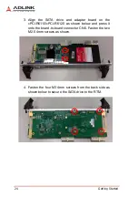
Page 34: ...rive and adapter board on the cPCI R6110 cPCI R6120 as shown below and press it onto the board to board connector CN6 Fasten the two M2 5 4mm screws as shown 4 Fasten the four M3 4mm screws from the b...

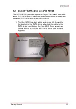
Page 35: ...tional 2 5 SATA drive Follow the instructions below to install the additional 2 5 SATA drive to the cPCI R6120 1 Find the SATA bracket cable and screw kit Assemble the bracket to the SATA drive attach...

Page 36: ...ding EDGE COMPUTING 2 Place the drive assembly onto the cPCI R6120 as shown below Insert the SATA connector into CN8 3 Fasten the four M3 8mm screws from the back side as shown below to secure the dri...

Page 37: ...Turn off power and unplug any power cords cables X To avoid electrical shock and or damage to equipment Z Keep equipment away from water or liquid sources Z Keep equipment away from high heat or high...

Page 38: ...must be serviced by authorized technicians when Z The power cord or plug is damaged Z Liquid has penetrated the equipment Z It has been exposed to high humidity moisture Z It is not functioning or doe...

Page 39: ...408 360 0200 Toll Free 1 800 966 5200 USA only Fax 1 408 360 0222 Email info adlinktech com ADLINK Technology China Co Ltd 300 Fang Chun Rd Zhangjiang Hi Tech Park Pudong New Area Shanghai 201203 Chin...

Reviews: