background image

Connectors

 11

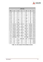
J2 (64-bit)

Pin

A

B

C

D

E

F

J2-22

NC

NC

NC

NC

NC

GND

J2-21

NC

NC

NC

NC

NC

GND

J2-20

NC

NC

NC

GND

NC

GND

J2-19

NC

NC

NC

NC

NC

GND

J2-18

NC

NC

NC

GND

NC

GND

J2-17

NC

GND

NC

NC

NC

GND

J2-16

NC

NC

NC

GND

NC

GND

J2-15

NC

GND

NC

NC

NC

GND

J2-14

AD[35]

AD[34]

AD[33]

GND

AD[32]

GND

J2-13

AD[38]

GND

VIO

AD[37]

AD[36]

GND

J2-12

AD[42]

AD[41]

AD[40]

GND

AD[39]

GND

J2-11

AD[45]

GND

VIO

AD[44]

AD[43]

GND

J2-10

AD[49]

AD[48]

AD[47] GND

AD[46]

GND

J2-9

AD[52]

GND

VIO

AD[51]

AD[50]

GND

J2-8

AD[56]

AD[55]

AD[54]

GND

AD[53]

GND

J2-7

AD[59]

GND

VIO

AD[58]

AD[57]

GND

J2-6

AD[63]

AD[62]

AD[61]

GND

AD[60]

GND

J2-5

C/BE[5]#

GND

VIO

C/BE[4]#

PAR64

GND

J2-4

VIO

NC

C/BE[7]#

GND

C/BE[6]# GND

J2-3

NC

GND

NC

NC

NC

GND

J2-2

NC

NC

NC

NC

NC

GND

J2-1

NC

GND

NC

NC

NC

GND

Table  2-4: J2 Connector Pin Definitions (64-bit)

Summary of Contents for cPCI-8301

Page 1: ...Advance Technologies Automate the World Manual Rev 2 00 Revision Date November 1 2004 Part No 50 15024 100 cPCI 8301 3U CompactPCI 64 bit PMC Carrier Board User s Manual...

Page 2: ...tial damages arising out of the use or inability to use the product or documentation even if advised of the possibility of such damages This document contains proprietary information protected by copy...

Page 3: ...ice adlinktech com TEL 886 2 82265877 FAX 886 2 82265717 Address 9F No 166 Jian Yi Road Chungho City Taipei 235 Taiwan Please email or FAX this completed service form for prompt and satisfactory servi...

Page 4: ......

Page 5: ...duction 1 1 1 Product Overview 1 1 2 Unpacking Checklist 2 1 3 cPCI 8301 Mechanical Drawing 3 1 4 cPCI 8301 Functional Diagram 4 1 5 cPCI 8301 Placement 4 1 6 Number of Boards Supported per PCI Bus 5...

Page 6: ...Tables List of Tables Table 2 1 P1 and P2 PMC Connector Pin Definitions 7 Table 2 2 P3 PMC Connector Pin Definitions 8 Table 2 3 J1 Connector Pin Definitions 10 Table 2 4 J2 Connector Pin Definitions...

Page 7: ...List of Figures iii List of Figures Figure 1 1 cPCI 8301 Carrier Board Layout 3 Figure 1 2 cPCI 8301 Functional Diagram 4 Figure 1 3 cPCI 8301 Top View 4 Figure 1 4 cPCI 8301 Bottom View 5...

Page 8: ...iv...

Page 9: ...e PMC site It supports 32 64 bit 33 66MHz PCI buses It is PICMG 2 0 CompactPCI Specification R2 1 and IEEE 1386 1 PMC Standard compliant Note There is no VIO keying on the cPCI 8301 VIO is directly co...

Page 10: ...e if there are any items missing please contact your dealer Included Items cPCI 8301 carrier board This manual Note The packaging of the cPCI 8301 OEM version with non standard configuration functiona...

Page 11: ...Introduction 3 1 3 cPCI 8301 Mechanical Drawing Figure 1 1 cPCI 8301 Carrier Board Layout...

Page 12: ...4 Introduction 1 4 cPCI 8301 Functional Diagram Figure 1 2 cPCI 8301 Functional Diagram 1 5 cPCI 8301 Placement Figure 1 3 cPCI 8301 Top View...

Page 13: ...t can be supported on one PCI bus is dependant on the frequency of the PMC cards installed Please refer to the following table Note If one or more 33MHz PMC cards is installed all cards will run at 33...

Page 14: ...6 Introduction...

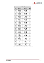
Page 15: ...K 12V 2 1 12V TRST 2 3 GND INTA 4 3 TMS TDO 4 5 INTB INTC 6 5 TDI GND 6 7 NC 5V 8 7 GND NC 8 9 INTD NC 10 9 NC NC 10 11 GND NC 12 11 BUSMODE2 3 3V 12 13 CLK GND 14 13 RST BUSMODE3 14 15 GND GNT 16 15...

Page 16: ...D 05 54 53 3 3V NC 54 55 AD 04 GND 56 55 PMC RSVD1 GND 56 57 V I O AD 03 58 57 PMC RSVD2 PMC RSVD3 58 59 AD 02 AD 01 60 59 GND PMC RSVD4 60 61 AD 00 5V 62 61 ACK64 3 3V 62 63 GND REQ64 64 63 GND NC 64...

Page 17: ...GND 32 33 GND AD 48 34 35 AD 47 AD 46 36 37 AD 45 GND 38 39 V I O AD 44 40 41 AD 43 AD 42 42 43 AD 41 GND 44 45 GND AD 40 46 47 AD 39 AD 38 48 49 AD 37 GND 50 51 GND AD 36 52 53 AD 35 AD 34 54 55 AD...

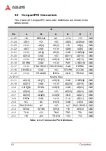
Page 18: ...18 SERR GND 3 3V PAR C BE 1 GND J1 17 3 3V PMC RSVD3 PMC RSVD4 GND PERR GND J1 16 DEVSEL GND VIO STOP LOCK GND J1 15 3 3V FRAME IRDY GND TRDY GND J1 12 14 Keying Area J1 11 AD 18 AD 17 AD 16 GND C BE...

Page 19: ...J2 13 AD 38 GND VIO AD 37 AD 36 GND J2 12 AD 42 AD 41 AD 40 GND AD 39 GND J2 11 AD 45 GND VIO AD 44 AD 43 GND J2 10 AD 49 AD 48 AD 47 GND AD 46 GND J2 9 AD 52 GND VIO AD 51 AD 50 GND J2 8 AD 56 AD 55...

Page 20: ...12 Connectors...

Page 21: ...anufactured by ADLINK will be covered by the original manufacturers warranty XFor products containing storage devices hard drives flash cards etc please back up your data before send ing them for repa...

Page 22: ...als XDamage caused by leakage of battery fluid during or after change of batteries by customer user XDamage from improper repair by unauthorized techni cians XProducts with altered and or damaged seri...

Reviews: