background image


32

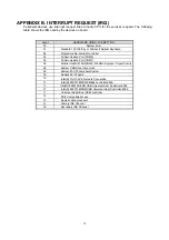
APPENDIX B. INTERRUPT REQUEST (IRQ) 

Peripheral devices use interrupt request lines to notify CPU for the services required. The following 
table shows the IRQ used by the devices on board. 


Level 

HARDWARE USING THE SETTING 

00 System 

timer 

01 

Standard 101/102-Key or Microsoft Natural Keyboard 

02 

Programmable interrupt controller 

03 

Communication Port (COM2) 

04 

Communication Port (COM1) 

05 

Mobile Intel(R) 915GM/GMS, 915GML Express Chipset Family 

08 

System CMOS/real time clock 

09 

Microsoft ACPI-Compliant System 

09 

Realtek AC’97 Audio 

10 

Intel(R) Pro/100 VE Network Connection 

11 

Intel(R) 82801FB/FBM SMBus controller-266A 

11 

Intel(R) 82801FB/FBM USB Universal Host Controller-2658 

11 

Intel(R) 82801FB/FBM USB Universal Host Controller-2659 

11 

Universal Serial Bus (USB) controller 

12 

PS/2 Compatible Mouse 

13 

Numeric data processor 

14 

Primary IDE Channel 

15 

Secondary IDE Channel 

Summary of Contents for AR-B1842-G

Page 1: ...AR B1842 G Socket 479 Pentium M INDUSTRIAL GRADE CPU BOARD User s Guide Edition 2 01 Book Number AR B1842 07 0115...

Page 2: ...L PORT HEADER J2 13 3 12 CPU FREQUENCY SELECT TABLE J10 13 3 13 HARD DISK CONNECTOR IDE1 13 3 14 COMPACT FLASH CONNECTOR CF1 14 3 15 COMPACT FLASH CONNECTOR MASTER SLAVE SELECT HEADER JP6 14 3 16 AUDI...

Page 3: ...uide if you have not already installed this AR B1842 G Check the packing list before you install and make sure the accessories are completely included AR B1842 G CD provides the newest information reg...

Page 4: ...components Although areas with humid climates are much less prone to static build up it is always best to safeguard against accidents that may result in expensive repairs The following measures should...

Page 5: ...II SO DIMM sockets supports up to 1GB of memory Two Serial and two SATA ports are supported There is one IDE connectors IDE1 supporting UDMA33 66 100 while supporting a CF Type II socket for its slave...

Page 6: ...GMA CRT 1 x VGA port D Sub15 LVDS 18 bits LVDS Interface LCD inverter power connector and ON OFF control Support 3 3V DF13 Audio Audio Interface AC97 Codec Realtek ALC 655 Line out L R Channel Storage...

Page 7: ...2801FBM USB2 0 8 Dothan Processor DMI direction media interface Serial ATA x2 Intel U21 82562ET LVDS DUAL CH Com1 RS232 1257 PCBGA Com2 RS232 LAN Diff 7 PCI E Bus 3 Express port LVDS 9 single 1GB pin...

Page 8: ...stall the AR B1842 G At first the layout of AR B1842 G is shown and the unpacking information that you should be careful is described The jumpers and switches setting for the AR B1842 G s configuratio...

Page 9: ...eft picture below loosen the screw first before inserting the processor Place the processor into the socket by making sure the notch on the corner of the CPU corresponds with the notch on the inside o...

Page 10: ...the DDR2 module so that the key of the DDR2 module align with those on the memory slot 2 Gently push the DDR2 module in an upright position until the clips of the slot close to hold the DDR2 module i...

Page 11: ...YBOARD MOUSE CN1 3 2 KEYBOARD MOUSE HEADER J6 3 3 KEYBOARD LUCK UNLCK HEADER JP5 3 4 SERIAL PORT CONNECTOR COM1 3 5 INTERNAL SERIAL PORT HEADER COM2 PIN SIGNAL PIN SIGNAL 1 KBDAT 2 MSDAT 3 GND 4 5V 5...

Page 12: ...R LAN1 PIN SIGNAL 1 2 ON RS232 Factory Preset 3 4 ON RS422 5 6 ON RS485 PIN SIGNAL 1 TX2 2 TX2 3 RX2 4 RX2 PIN SIGNAL PIN SIGNAL 1 5V 2 N C 3 IRRX 4 GND 5 IRTX PIN SIGNAL PIN SIGNAL 1 RED 9 VCC 2 GREE...

Page 13: ...PE 25 GND 13 SLCT 26 N C PIN CPU_HOST_FREQUENCY 4_6 1_3 100MHz BANIAS 4_6 3_5 133MHz DOTHAN PIN SIGNAL PIN SIGNAL 1 RESET 2 GND 3 PDATA7 4 PDATA8 5 PDATA6 6 PDATA9 7 PDATA5 8 PDATA10 9 PDATA4 10 PDAT...

Page 14: ...DATA4 4 SDATA5 5 PDATA6 6 SDATA7 7 PDCS1 8 GND 9 GND 10 GND 11 GND 12 GND 13 5V 14 GND 15 GND 16 GND 17 GND 18 PDA2 19 PDA1 20 PDA0 21 PDATA0 22 PDATA1 23 PDATA2 24 GND 25 GND 26 GND 27 PDATA11 28 PDA...

Page 15: ...AL OPERATION Factory Preset 2 3 ON CLEAR CMOS PIN SIGNAL PIN SIGNAL 1 LVDS_PWR 2 GND 3 LVDS_CLKBN 4 LVDS_CLKBP 5 GND 6 LVDS_YBN2 7 LVDS_YBP2 8 GND 9 LVDS_YBN1 10 LVDS_YBP1 11 N C 12 N C 13 LVDS_YBP0 1...

Page 16: ...CPU VOLTAGE SELECT HEADER JP1 1 PIN SIGNAL PIN SIGNAL 1 VCC 5 GND 2 DATA 6 DATA 3 DATA 7 DATA 4 GND 8 VCC PIN SIGNAL PIN SIGNAL 1 GND 5 SATA RXP 2 SATATXP 6 SATARXN 3 SATATXN 7 GND 4 GND PIN SIGNAL PI...

Page 17: ...HEADER JP2 1 3 3 29 PANEL HEADER J3 3 30 AT POWER CONNECTOR PW1 PIN SIGNAL 1 2 ON WRITER FUNCTION 2 3 ON READ FUNCTION Factory Preset PIN SIGNAL 1 2 POWER LED 3 4 HDD LED 5 6 SPEAKER 7 8 RESET BUTTON...

Page 18: ...abled the watchdog timer your program should trigger the watchdog timer every time before it times out After you trigger the watchdog timer the timer will be set to zero and start to count again If yo...

Page 19: ...Port_Address 1 0xFE outportb IO_Port_Address 0x07 Point to Logical Device Number Reg outportb IO_Port_Address 1 0x08 Select logical device 8 Watchdog Function outportb IO_Port_Address 0x30 Device Acti...

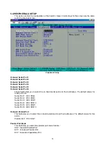
Page 20: ...t the system clock and error handling If the motherboard is already installed in a working system you will not need to select this option You will need to run this Setup option however if you change y...

Page 21: ...n manually You will be asked to enter the following items CYLS Number of cylinders HEAD Number of read write heads PRECOMP Write precompensation LANDING SONE Landing zone SECTOR Number of sectors The...

Page 22: ...Self Test When enabled this field speeds up the Power On Self Test POST after the system is turned on If it is set to Enable BIOS will skip some items USB Keyboard Support The options for this field...

Page 23: ...Enable this function to support ACPI Advance Configuration and Power Interface ACPI Suspend Type This options for this field are S1 POS and S3 STR By default the field is set to S1 POS PWRON After PW...

Page 24: ...n board serial ports and their addresses The default values for these ports are Serial Port 1 3F8 IRQ4 Serial Port 2 2F8 IRQ3 Serial Port 3 3E8 IRQ11 Serial Port 4 2E8 IRQ10 Serial Port 5 4F8 IRQ11 Se...

Page 25: ...r this field are Enabled and Disabled By default the field is set to Enabled In order to use USB 2 0 necessary OS drivers must be installed first Please update your system to Windows 2000 SP4 or Windo...

Page 26: ...set to this value PnP PCI Setup Reset Configuration Data Thus field allows you to determine whether to reset the configuration data or not The default value is Disabled Resources Controlled By This P...

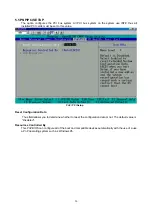
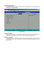
Page 27: ...parameters of the hardware monitoring function feature of the motherboard The values are read only values as monitored by the system and show the PC health status Shutdown Temperature This field allow...

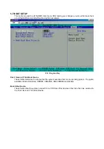
Page 28: ...s PCI Plug And Play First Second Third Boot Device These fields determine the device that the system searches first for an operating system The option available include Hard Disk CDROM USB FDD USB CDR...

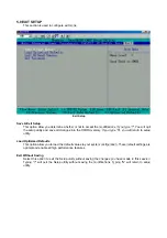
Page 29: ...you type N you will return to setup utility Load Optimized Defaults This option allow you to load the default values to your system configuration These default settings are optimal and enable all high...

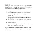
Page 30: ...on t turn off your computer during the flashing or it will damage your BIOS ROM Step 1 Turn on your system and don t detect the CONFIG SYS and AUTOEXEC BAT files Step 2 You will get AWDFLASH EXE and X...

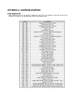
Page 31: ...BF Motherboard resources 00C0 00DF Direct Memory Access controller 00E0 00EF Motherboard resources 00F0 00FF Numeric data processor 0170 0177 Secondary IDE Channel 01F0 01F7 Primary IDE Channel 0274 0...

Page 32: ...unication Port COM2 04 Communication Port COM1 05 Mobile Intel R 915GM GMS 915GML Express Chipset Family 08 System CMOS real time clock 09 Microsoft ACPI Compliant System 09 Realtek AC 97 Audio 10 Int...

Reviews: