background image


TEAR OFF THE PASTIC FILM OF BEZEL AND 
PANEL AND CHECKING THE GAP WHETHER 
WRONG 
 
CHECKING THE OUTLINE OF LCD WHETHER 
SCRAPE AND DIRTY 
 
CHECKING GAP BETWEEN THE BEZEL AND 
REAR COVER WHETHER WRONG 


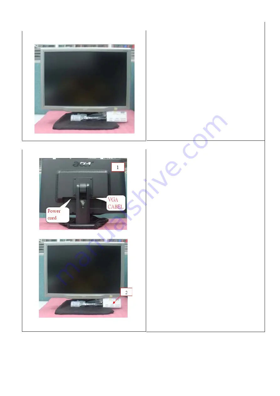
INSERT THE SIGNAL CABLE AND POWER 
CORD TO LCD AND SETTLE IT 
 
STICK FLOW CARD ON THE BEZEL 


All manuals and user guides at all-guides.com

Summary of Contents for X241W

Page 1: ...vice Guide Service guide files and updates are available on the CSD web for more information Please refer to http csd acer com tw 100 Recycled Paper All manuals and user guides at all guides com a l l g u i d e s c o m ...

Page 2: ...eof and specifically disclaims any warranties of merchantability or fitness for any particular purpose Any Acer Incorporated software described in this manual is sold or licensed as is Should the programs prove defective following their purchase the buyer and not Acer Incorporated its distributor of its dealer assumes the entire cost of all necessary servicing repair and any incidental or conseque...

Page 3: ...itional information related to the current topic Warning Alerts you to any damage that might result from doing or not doing specific actions Caution Gives precautionary measures to avoid possible hardware or software problems Important Reminds you to do specific actions relevant to the accomplishment of procedures All manuals and user guides at all guides com ...

Page 4: ...s generic service guide In such cases please contact your regional offices or the responsible personnel channel to provide you with further technical details 2 please not WHEN ORDERING FRU PARTS that you should check the most up to date information available on your regional web or channel If for whatever reason a part number change is made it will not be noted in the printed Service Guide for ACE...

Page 5: ...ase the separation between the equipment and receiver 3 Connect the equipment into an outlet on a circuit different from that to which the receiver is connected 4 Consult the dealer or an experienced radio TV technician for help NOTICE 1 The changes or modifications not expressly approved by the party responsible for compliance could void the user s authority to operate the equipment 2 Shielded in...

Page 6: ...a three pronged grounded plug a plug with a third grounding pin This plug will fit only into a grounded power outlet as a safety feature If your outlet does not accommodate the three wire plug have an electrician install the correct outlet or use an adapter to ground the appliance safely Do not defeat the safety purpose of the grounded plug z Unplug the unit during a lightning storm or when it wil...

Page 7: ... brightness in the screen depending on the desktop pattern you use z The LCD screen has effective pixels of 99 99 or more It may include blemishes of 0 01 or less such as a missing pixel or a pixel lit all of the time z Due to the nature of the LCD screen an afterimage of the previous screen may remain after switching the image when the same image is displayed for hours In this case the screen is ...

Page 8: ...r 2 OPERATING INSTRUTION 31 Chapter 3 MACHINE ASSEMBLY 37 Chapter 4 TROBLE SHOOTING 53 Chapter 5 CONNECTOR INFORMATION 56 Chapter 6 FRU LIST 58 Chapter 7 SCHEMATIC DIAGRAM 62 Chapter 8 POWER BOARD INFORMATION 70 All manuals and user guides at all guides com ...

Page 9: ... Colors Maximum Dot Clock 162MHz Max Resolution 1920x1200 60HZ Plug Play VESA FPMPMI ON Mode 90W EPA ENERGY STAY OFF Mode 2W Audio output Rated Power 2 0W rms Per channel Input Connector D Sub 15 pin DVI connector on DVI box Input Video Signal Analog 0 7Vp p 75OHM Horizontal 518 4 mm Screen Size Active Vertical 324 mm Power Source 90 264 Vac 47 63HZ Environmental Considerations Operating Temp 5 to...

Page 10: ...TER External Controls Contrast brightness Focus Clock H Position W Position Language OSD Color temperature OSD Position Timeout Auto Config Input Information Reset Exit Regulatory Compliance cUL FCC TUV CE TCO03 All manuals and user guides at all guides com ...

Page 11: ... 480 lines 12 678 480 lines V F P ms 0 384 12 lines 0 317 10 lines 0 086 3 lines 0 237 9 lines SYNC H V POLARITY Or SEP SYNC Y Y Y Y MODE NO 5 6 7 8 RESOLUTION 640 x 480 800 x 600 800 x 600 800 x 600 Dot clock MHz 31 5 36 40 49 5 f h 37 500kHz 35 16kHz 37 879kHz 46 875kHz H Total us 26 667 840 dots 28 44 1024 dots 26 40 1056 dots 21 333 1056dots H Sync us 2 032 64 dots 2 00 72 dots 3 200 128 dots ...

Page 12: ...line 0 062 3 lines 0 05 3 lines SYNC H V POLARITY SEP SYNC Y2 Y Y Y MODE NO 13 14 15 16 RESOLUTION 1024 x 768 1280 x 1024 1280 x 1024 1152 x 864 Dot clock MHz 78 75 108 135 108 f h 60 02kHz 63 981kHz 79 976KHz 67 5 KHz H Total us 16 66 1312 dots 15 630 1688 dots 12 504 1688 dots 14 815 1600 dots H Sync us 1 22 96 dots 1 037 112 dots 1 067 144 dots 1 185 128 dots H B P us 2 23 176 dots 2 296 248 do...

Page 13: ...ine 0 013 1 line 0 022 5 lines 0 063 3 lines SYNC H V POLARITY SEP SYNC Y Y Y Y MODE NO 21 22 23 24 RESOLUTION 1280 x 768 1360 x 768 1440 x 900 1440 x 900 Dot clock MHz 102 25 85 5 106 5 136 75 f h 60 289KHz 47 712KHz 55 935KHz 70 635KHz H Total us 16 587 1696dots 20 959 1792dots 17 878 1904dots 14 157 1936dots H Sync us 1 252 128 dots 1 31 112 dots 1 427 152 dots 1 112 152 dots H B P us 2 034 208...

Page 14: ...ctive us 11 487 1680 dots 25 126 848 dots 12 468 1920 dots H F P us 0 711 104 dots 0 474 16 dots 0 312 48 dots f v 59 954 Hz 60 Hz 59 950Hz V Total ms 16 679 1089 lines 16 667 517 lines 16 681 1235 lines V Sync ms 0 092 6 lines 0 258 8 lines 0 081 6 lines V B P ms 0 459 30 lines 0 741 23 lines 0 351 26 lines V Active ms 16 082 1050 lines 15 474 480 lines 16 208 1200 lines V F P ms 0 046 3 line 0 1...

Page 15: ...e Size DocumentNumber Rev Date Sheet of 02 Top Level 7 8 Saturday December24 2005 C2A SCHEMATIC1 PROJECT PROJECT WDTB Page 5 GM5861 FSCLK FSCLK FSDQS FSCKE FSALTRAS FSALTCAS FSALTWE FSBKSEL0 FSBKSEL1 RED BLUE GREEN BLUE GREEN RED SOG VGA_SCL VGA_SDA AHS AVS SVDATA 0 7 SVODD SVS SHS SVCLK MSTR_SDA MSTR_SCL FSDATA 0 31 FSADDR 0 11 DQS 0 3 RESET SVDV PBIAS PPWR VGA_CAB PWM0 PWM1 MUTE ADO_R ADO_L ADO_...

Page 16: ... 16 PCB CONDUCTOR VIEW Main Board All manuals and user guides at all guides com a l l g u i d e s c o m ...

Page 17: ...All manuals and user guides at all guides com ...

Page 18: ...All manuals and user guides at all guides com ...

Page 19: ...All manuals and user guides at all guides com ...

Page 20: ...All manuals and user guides at all guides com ...

Page 21: ...All manuals and user guides at all guides com a l l g u i d e s c o m ...

Page 22: ...All manuals and user guides at all guides com ...

Page 23: ...All manuals and user guides at all guides com ...

Page 24: ...All manuals and user guides at all guides com ...

Page 25: ...All manuals and user guides at all guides com ...

Page 26: ...Button Board All manuals and user guides at all guides com a l l g u i d e s c o m ...

Page 27: ...All manuals and user guides at all guides com ...

Page 28: ... 16 POWER BOARD All manuals and user guides at all guides com ...

Page 29: ...All manuals and user guides at all guides com ...

Page 30: ...All manuals and user guides at all guides com ...

Page 31: ... to exit a selection in OSD 3 Left Plus If OSD is active press to select or adjust OSD options If OSD is inactive press once then press the buttons marked or to adjust the volume 4 Right Plus If OSD is active press to select or adjust OSD options If OSD is inactive press once then press the buttons marked or to adjust the volume 5 AUTO If OSD is active press to enter a selection in OSD If OSD is i...

Page 32: ...any vertical stripes seen on the background of the screen this renders them less noticeable by minimizing their size It also changes the size of the horizontal screen H Position This adjusts the horizontal V Position This adjusts the vertical Color adjustment There are three ways to adjust color Warm reddish white Cool bluish white User you can adjust the colors red green and blue to the intensity...

Page 33: ...nd Japanese Language for EMEA Select the OSD menu language Select from English German Spanish Russia Nederlands French Italian and Finnish OSD Settings This changes the position of the OSD window on the screen and the staying time Input signal Select either Analog Input or Digital Input video All manuals and user guides at all guides com ...

Page 34: ...Information This shows information about the screen Reset Resets all settings to default levels Exit Exit from OSD All manuals and user guides at all guides com ...

Page 35: ...VESA DDC STANDARD It allows the monitor to inform the host system of its identity and depending on the level of DDC used communicate additional information about its display capabilities The communication channel is defined in two levels DDC2B The DDC2B is a bi directional data channel based on the I2 C protocol The host can request EDID information over the DDC2B channel System in power off mode ...

Page 36: ...ally redrawn The appearance is similar to a Screen Saver feature except the display is completely off The display is restored by pressing a key on the keyboard or clicking the mouse USING THE RIGHT POWER CORD The accessory power cord for the Northern American region is the wallet plug with NEMA 5 15 style and is UL listed and CSA labeled The voltage rating for the power cord shall be 125 volt AC S...

Page 37: ...e different components vary in size During the disassembly process group the screws with the corresponding to avoid mismatch when putting back the components 2 Note The monitor surface is susceptible to scratching Therefore lay the monitor on a soft surface when mounting or removing the base 3 Wear gloves Front View unit mm All manuals and user guides at all guides com ...

Page 38: ... 38 Real View Top View All manuals and user guides at all guides com ...

Page 39: ... 39 Side View unit mm All manuals and user guides at all guides com ...

Page 40: ...RT THE M B CABLE TO THE SINK OF M B THEN PUT IT TO THE PRODUCTION LINE CONNECT THE POWER BOARD AND MAIN BOARD AND PUT THE TO SHIELDING SCAN THE FLOW CARD AND POWER BOARD CODE 2 ASSEMBLY PROCESS All manuals and user guides at all guides com ...

Page 41: ...0 8 B WITH INV B AS LEFT SHOW PUT THE POWER MYLAR TO THE SHIELDING LOCK UP 3 PCS SCREW F3 6T WITH MAIN BOARD AS LEFT SHOW GET THE INVERTER BOARD CABLE AND CHECKING INSERT THE CABLE TO THE SINK OF INVERTER BOARD All manuals and user guides at all guides com a l l g u i d e s c o m ...

Page 42: ...THE FLOW CARD AND INVERTER BOARD CODE PUT 2 PCS BRACKET TO THE INVERTER BOARD LOCK UP 4 PCS SCREWS M4 0 6 B TO THE INVERTER BOARD AS LEFT SHOW MOVE THE INVERTER BOARD TO THE FRONT OF PRODUCTION LINE PUT THE PANEL TO THE PRODUCTION LINE TEAR OFF THE PLASTIC FILM All manuals and user guides at all guides com ...

Page 43: ...TICK GOOEY ON THE PLASTIC FILM FOR FIXING TURN OVER THE LCD AND TEAR OFF THE GOOEY OF CCFT CABLE SCAN THE FLOW CARD THE PANEL CODE STICK 1 PCS FLOW CODE ON THE PANEL AS LEFT SHOW INSERT THE UPSIDE LAMP CABLE TO THE INVERTER BOARD All manuals and user guides at all guides com ...

Page 44: ...IDE LAMP CABLE TO THE INVERTER BOARD PUT THE LEFT BRACKET TO THE INVERTER BOARD LOCK UP 4 PCS F3 6 T WITH BRACKET LOCK UP 2 PCS M3 4 I WITH THE LEFT BRACKET LOCK UP 2 PCS M3 4 I WITH LEFT BRACKET TURN OVER THE LCD All manuals and user guides at all guides com ...

Page 45: ...GET THE BEZEL AND CHECKING PUT THE BEZEL TO THE PANEL STICK PLASTIC FILM ON THE BEZEL TURN OVER THE LCD All manuals and user guides at all guides com ...

Page 46: ...T SIDE BEZEL PUT 1 PCS FASTENER TO THE PANEL BACKSIDE LOCK UP3 PCS SCREWS M3 4 I TO THE LEFT SIDE BEZEL INSERT THE LVDS CABLE TO THE SINK OF LCD PUT THE SHIELDING ON THE LCD All manuals and user guides at all guides com a l l g u i d e s c o m ...

Page 47: ...EY ON THE SINK OF LVDS CABLE LOCK UP4 PCS SCREWS WITH THE SHEILDING AND BRACKET PUT THE FASTENERS TO BOTH SIDES OF LCD LOCK UP 4 PCS F3 10 B TO BOTH SIDES FOR FIXING All manuals and user guides at all guides com ...

Page 48: ...BUTTON BOARD PUT THE BUTTON BOARD TO THE BEZEL AND INSERT CABLE TO IT STICK 1 PCS AL FOIL TO THE BRACKET AS LEFT SHOW STICK 1 PCS AL FOIL TO THE SHIELDING AS LEFT SHOW INSERT THE INVERTER BOARD CABLE TO THE POWER BOARD All manuals and user guides at all guides com ...

Page 49: ... FOIL ON THE SHIELDING AS LEFT SHOW STICK 1 PCS AL FOIL TO THE BRACKET AS LEFT SHOW STICK 1 PCS AL FOIL TO THE SHIELDING AS LEFT SHOW PUT THE CABLE TO THE FASTENER AND STICK 1 PCS GOOEY ON THE LOCATION AS LEFT SHOW All manuals and user guides at all guides com ...

Page 50: ...ETTLED ROCK THE LCD WHETHER ANY DIFFERENT THINGS GET THE REAR COVER AND CHECKING PUT THE REAR COVER TO THE BEZEL STICK 1 PCS GOOEY TO THE REAR COVER AS LEFT SHOW LOCK UP 2 PCS SCREWS TO THE BEZEL AND REAR COVER FOR FIXING GET THE STANDS AND CHECKING STICK 1 PCS FLOW CODE ON THE REAR COVER All manuals and user guides at all guides com ...

Page 51: ... UP 4 PCS SCREWS M4 10 B TO THE REAR COVER FOR FIXING GET THE BASE AND CHECKING PUT THE BASE TO THE STAND OF REAR COVER PUT THE BAG OF TOOL TO THE BASE STAND UP THE LCD AND PUT OUT THE FOAM All manuals and user guides at all guides com a l l g u i d e s c o m ...

Page 52: ...AP WHETHER WRONG CHECKING THE OUTLINE OF LCD WHETHER SCRAPE AND DIRTY CHECKING GAP BETWEEN THE BEZEL AND REAR COVER WHETHER WRONG INSERT THE SIGNAL CABLE AND POWER CORD TO LCD AND SETTLE IT STICK FLOW CARD ON THE BEZEL All manuals and user guides at all guides com ...

Page 53: ...Check U13 1 8V U12 3 3V Change U13 U12 NO Check Short Of Main Board No Yes Check X1 14 318MHz NO Change X1 or U4 Yes Check U8 Pin 1 2 5 6 Clock NO Change U7 or RUN Software ISP Change U7 Yes Check Key Board Yes Change Key Board NO Chapter 4 All manuals and user guides at all guides com ...

Page 54: ...DVI Cable Yes Change Cable NO Check R4 R8 R10 Change R4 R8 R10 U 7 NO Yes Check CN5 LVDS Signal NO Change U7 or CN5 Cable or Panel Yes Check OSD R G B Gain NO Adjustment R G B Color Change Panel Yes All manuals and user guides at all guides com ...

Page 55: ...or DVI Cable Yes Change Cable NO VGA Check R4 R8 R10 R20 R21 Change VGA Cable or R4 R8 R10 R20 R21 or U7 NO DVI Check U7 Pin 109 110 112 113 117 118 120 121 Change DVI Cable or U7 Yes Change U7 NO Yes All manuals and user guides at all guides com ...

Page 56: ...io Line in receptacle Video signal connector 15P Mini D Sub connector x 1 PIN Signal 1 Red 2 Green 3 Blue 4 No Pin 5 Ground 6 Ground Red 7 Ground Green 8 Ground Blue 9 5 V for DDC 10 Ground 11 Ground 12 SDA DDC Data 13 H Sync 14 V Sync 15 SCL DDC Clock All manuals and user guides at all guides com a l l g u i d e s c o m ...

Page 57: ... TMDS data2 shield 4 NC 5 NC 6 DDC clock 7 DDC data 8 Not connected 9 TMDS data1 10 TMDS data1 11 TMDS data1 shield 12 NC 13 NC 14 5V 15 Ground return for 5 V and H V sync 16 Hot plug detect 17 TMDS data0 18 TMDS data0 19 TMDS data0 shield 20 NC 21 NC 22 TMDS clock shield 23 TMDS clock 24 TMDS clock All manuals and user guides at all guides com ...

Page 58: ...reasons a part number change is made it will not be noted in the printed Service Guide For ACER AUTHORIZED CERVICE PROVIDERS your Acer office may have a DIFFERENT part number code to those given in the FRU list of this printed Service Guide You MUST use the local FRU list provided by your regional Acer office to order FRU parts repair and service of customer machines NOTE To scrap or to return the...

Page 59: ...EXPLODED VIEW All manuals and user guides at all guides com ...

Page 60: ... GP 1 30 EAL0TB03014 STAND L0TB G 10 FCWDTB01014 BKT L MYLAR WDTB GP 1 31 EBL9TB02013 HINGE COVER 11 FBWDTB03016 BKT L PLATE WDTB GP 2 32 FAWDTB02019 HINGE ASSY W 12 FBWDTB02010 LCD BKT R WDTB GP 1 33 MF40080IBJ1 SCREW F4 0 8 13 EBL70023013 WIRE MOUNTS L70L E GP 1 34 EAWDTB03015 STANDARD BA 14 FCWDTB02011 INVERTOR MYLAR WDTB GP 1 35 GAL7TA01016 RUBBER FOOT 15 FCM7T004014 AL FOIL M7T GP 4 36 FBWDTB...

Page 61: ...cription of the following component Item Picture Description Part No 1 back cover 25WDTBLC001 2 bezel 34WDTBLB004 3 base 38WDTBBS006 4 stand 37WDTBSU007 5 screw MM40080BBW1 All manuals and user guides at all guides com a l l g u i d e s c o m ...

Page 62: ...XGA LCD Controller Board Design Genesis 5861 RD1 Date Date CONTENTS 1 Comments 06 POWER KEYPAD 03 GRAPHIC INPUT 02 CONTENTS A Author Position 01 Cover Page XXXXX 05 SDRAM AMP OUTPUT Initial Release Signature 07 History 6 2005 11 2 3 Ver 4 SHEET SCHEMATIC DIAGRAM All manuals and user guides at all guides com ...

Page 63: ...3pF C3 75R 1 C3 75R 1 C30 0 1uF C30 0 1uF C35 33pF NC C35 33pF NC R53 75R 1 R53 75R 1 D14 DAN217K NC D14 DAN217K NC 1 2 3 PAD1 EMI PAD PAD1 EMI PAD C200 0 1uF NC C200 0 1uF NC C39 0 1uF C39 0 1uF U18 SN74LVC14A NC U18 SN74LVC14A NC GND 7 VCC 14 6A 13 6Y 12 5A 11 5Y 10 1A 1 1Y 2 2A 3 2Y 4 3Y 6 3A 5 4Y 8 4A 9 D7 DAN217K NC D7 DAN217K NC 1 2 3 R25 R25 C2 75R 1 C2 75R 1 R60 4K7 R60 4K7 R33 10K R33 10K...

Page 64: ...1uF C60 0 1uF R238 10K R238 10K C51 0 1uF C51 0 1uF C62 0 1uF C62 0 1uF R109 10K R109 10K CN3 AMP 640456 4 CN3 AMP 640456 4 1 2 3 4 R248 0R NC R248 0R NC C81 47uF 10V C81 47uF 10V U7 GM5861 U7 GM5861 DQ15_A 8 DQ6_A 1 DQ5_A 2 DQ4_A 3 DQ3_A 4 DQ2_A 5 DQ1_A 6 DQ0_A 7 DQ14_A 9 DQ13_A 10 DQ12_A 11 DQ11_A 12 DQ10_A 13 DQ9_A 14 DQ8_A 15 CRVSS 16 RVDD_3 3 17 WE 18 CAS 19 RAS 20 BA 21 MCLK 22 A9 23 CRVSS 2...

Page 65: ...5 VSS 26 A4 27 A5 28 A6 29 A7 30 A8 31 A9 32 NC 33 CKE 34 CLK 35 UDQM 36 NC 37 VDDQ 38 DQ8 39 DQ9 40 VSSQ 41 DQ10 42 DQ11 43 VDDQ 44 DQ12 45 DQ13 46 VSSQ 47 DQ14 48 DQ15 49 VSS 50 C142 0 1uF C142 0 1uF C154 0 1uF C154 0 1uF R217 0R R217 0R C126 1nF C126 1nF C158 1nF C158 1nF C135 0 01uF C135 0 01uF FB14 L1206 FB14 L1206 R132 150K R132 150K R152 10K NC R152 10K NC R169 4K7 NC R169 4K7 NC C129 0 1uF...

Page 66: ...1206 NC R187 100R R187 100R R198 100R NC R198 100R NC R193 100R R193 100R 1 H3 MTH276D126 1 H3 MTH276D126 2 3 4 5 6 7 8 9 D19 SSM54PT D19 SSM54PT C A C192 0 1uF C192 0 1uF R191 100R R191 100R Q16 MMST3906 NC Q16 MMST3906 NC C207 0 1uF 6 C207 0 1uF 6 R233 4K7 NC R233 4K7 NC C201 100uF 25V C201 100uF 25V R179 2K2 R179 2K2 C175 0 1uF C175 0 1uF C173 0 1uF C173 0 1uF U15 AIC1563 U15 AIC1563 SC 1 SE 2 ...

Page 67: ...mber Date L7TB L Key Board PROJECT NA L7TB L9TB A Monday October 31 POWER MENU AUTO RIGHT LEFT AMBER GREEN SW1 TOUCH SWITCH 4P SW1 TOUCH SWITCH 4P 1 2 3 LD1 LED Dual LD1 LED Dual SW5 TOUCH SWITCH 4P SW5 TOUCH SWITCH 4P 1 2 3 4 5 6 7 8 CN8 JST 8Pin PH2 0mm H CN8 JST 8Pin PH2 0mm H 1 2 3 LD2 LED Dual LD2 LED Dual SW4 TOUCH SWITCH 4P SW4 TOUCH SWITCH 4P SW3 TOUCH SWITCH 4P SW3 TOUCH SWITCH 4P SW2 TOU...

Page 68: ...64S IC1 C6 R6 R7 WJ1 R8 C7 C8 R16 C9 C10 C11 C12 R18 R19 R20 R5 C13 R13 R14 R12 R9 F2 C3 R21 Vadj CR2 CR3 R35 R36 C24 C25 R31 R32 R33 R34 C26 C27 C28 CR4 CR5 R48 R49 C43 C44 C37 C38 C39 F E C23 1 2 3 4 5 6 7 8 Q4 1 2 3 4 5 6 7 8 Q5 C2 C4 1 2 3 4 5 6 7 8 Q6 1 2 3 4 5 6 7 8 Q7 C30 C31 A B D C B A C36 R10 WJ3 C32 WJ2 E F A B C A B D C48 WJ4 R11 R17 CR34 Q8 R15 R22 G R23 G D S Q9 CR35 R25 1 2 3 4 5 6 ...

Page 69: ... 檢圖 CHECKED 承認 APPVD 日 DA 日 日 DA 日 DA 日 DA 3DA01306X F101 C101 CR101 CR102 R105 R106 C108 C109 C110 C111 C112 9 7 1 5 T103 9 7 1 5 T101 9 7 1 5 T102 9 7 1 5 T104 VIN 1 2 3 4 5 6 7 8 Q105 1 2 3 4 5 6 7 8 Q106 C105 C106 A B C D VIN A B C D C100 R100 C102 R101 C103 R102 C104 R103 H H B A C D H CR10 CR10 CR10 CR11 CR108 CR109 All manuals and user guides at all guides com ...

Page 70: ...Power Board Current set Information Power Board AS08B360411 P N Model Name AS08B360411 AS08B360411 FSP112 3F01 T43 90 240V NO Jump All manuals and user guides at all guides com ...

Reviews: