4-8
Theory of Operation
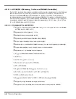
4.2.3.1 ALI M1521 (Memory, Cache and DRAM Controller)
The M1521 provides the system controller and data path components for the Extensa
900 Pentium-based system. It provides 64-bit CPU bus interface, 32-bit PCI bus
interface, 64/72 DRAM data bus with ECC or parity, secondary cache interface
including pipeline burst SRAM or asynchronous SRAM, PCI master to DRAM interface,
four PCI master arbiters, and a UMA arbiter. The M1521 bus interfaces are designed
to interface with 3V and 5V buses. It directly connects to 3V CPU bus, 3V or 5V tag,
3V or 5V DRAM bus, and 5V PCI bus.
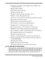
4.2.3.1.1 Features of the ALI M1521
♦
Supports all Intel/Cyrix
®
/AMD 586-class processors (with host bus of 66 MHz,
60 MHz and 50 MHz at 3V)
♦
Supports M1/K5/Dakota™ CPUs
♦
Supports linear wrap mode for M1
♦
Supports asynchronous/pipeline-burst SRAM
♦
Write-back/dynamic write-back cache policy
♦
Built-in 8K* 2-bit SRAM for MESI protocol to cost and enhance performance
♦
Cacheable memory up to 512 MB with 11-bit tag SRAM
♦
Supports 3V/5V SRAMs for tag address
♦
Supports FPM/EDO/BEDO/SDRAM DRAMs
♦
RAS lines
♦
64-bit data path to memory
♦
Symmetrical/asymmetrical DRAMs
♦
3V or 5V DRAMs
♦
Duplicated MA[1:0] driving pins for burst access
♦
No buffer needed for RASJ and CASJ and MA[1:0]
♦
CBR and RAS-only refresh
♦
Supports 64M-bit (16M* 4, 8M* 8, 4M*16) technology DRAMs
♦
Supports programmable-strength MA buffer
♦
Supports error checking and correction (ECC) and parity for DRAM
Summary of Contents for Extensa 900 Series
Page 1: ...Maintenance Manual ExtensaTM 900 Series Notebook Computers 9813715 0001 December 1996 ...
Page 10: ......
Page 28: ......
Page 44: ......
Page 56: ......
Page 82: ......
Page 98: ......
Page 138: ...A 2 Notebook Schematic Diagrams Figure A 1 Notebook Main Board Logic Diagrams Sheet 1 of 30 ...
Page 139: ...Notebook Schematic Diagrams A 3 Figure A 1 Notebook Main Board Logic Diagrams Sheet 2 of 30 ...
Page 140: ...A 4 Notebook Schematic Diagrams Figure A 1 Notebook Main Board Logic Diagrams Sheet 3 of 30 ...
Page 141: ...Notebook Schematic Diagrams A 5 Figure A 1 Notebook Main Board Logic Diagrams Sheet 4 of 30 ...
Page 142: ...A 6 Notebook Schematic Diagrams Figure A 1 Notebook Main Board Logic Diagrams Sheet 5 of 30 ...
Page 143: ...Notebook Schematic Diagrams A 7 Figure A 1 Notebook Main Board Logic Diagrams Sheet 6 of 30 ...
Page 145: ...Notebook Schematic Diagrams A 9 Figure A 1 Notebook Main Board Logic Diagrams Sheet 8 of 30 ...
Page 146: ...A 10 Notebook Schematic Diagrams Figure A 1 Notebook Main Board Logic Diagrams Sheet 9 of 30 ...
Page 147: ...Notebook Schematic Diagrams A 11 Figure A 1 Notebook Main Board Logic Diagrams Sheet 10 of 30 ...
Page 148: ...A 12 Notebook Schematic Diagrams Figure A 1 Motherboard PWB Logic Diagrams Sheet 11 of 23 ...
Page 149: ...Notebook Schematic Diagrams A 13 Figure A 1 Notebook Main Board Logic Diagrams Sheet 12 of 30 ...
Page 153: ...Notebook Schematic Diagrams A 17 Figure A 1 Notebook Main Board Logic Diagrams Sheet 16 of 30 ...
Page 154: ...A 18 Notebook Schematic Diagrams Figure A 1 Notebook Main Board Logic Diagrams Sheet 17 of 30 ...
Page 155: ...Notebook Schematic Diagrams A 19 Figure A 1 Notebook Main Board Logic Diagrams Sheet 18 of 30 ...
Page 156: ...A 20 Notebook Schematic Diagrams Figure A 1 Notebook Main Board Logic Diagrams Sheet 19 of 30 ...
Page 157: ...Notebook Schematic Diagrams A 21 Figure A 1 Notebook Main Board Logic Diagrams Sheet 20 of 30 ...
Page 158: ...A 22 Notebook Schematic Diagrams Figure A 1 Notebook Main Board Logic Diagrams Sheet 21 of 30 ...
Page 159: ...Notebook Schematic Diagrams A 23 Figure A 1 Notebook Main Board Logic Diagrams Sheet 22 of 30 ...
Page 160: ...A 24 Notebook Schematic Diagrams Figure A 1 Notebook Main Board Logic Diagrams Sheet 23 of 30 ...
Page 161: ...Notebook Schematic Diagrams A 25 Figure A 1 Notebook Main Board Logic Diagrams Sheet 24 of 30 ...
Page 166: ...A 30 Notebook Schematic Diagrams Figure A 1 Notebook Main Board Logic Diagrams Sheet 29 of 30 ...
Page 168: ......
Page 171: ...MPB Schematic Diagrams B 3 Figure B 1 MPB CPU Board Logic Diagrams Sheet 2 of 3 ...
Page 176: ...B 8 MPB Schematic Diagrams Figure B 3 MPB Main Board Motherboard Logic Diagrams Sheet 3 of 10 ...
Page 196: ......
Page 197: ......
Page 198: ......

