MC96FM204/FM214
80
April 7, 2016 Ver. 1.8
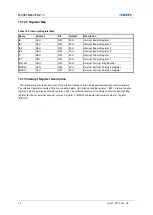
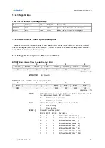
11.1.3 Register Map
Table 11-1 Clock Generator Register Map
Name
Address
Dir
Default
Description
SCCR
8AH
R/W
00H
System and Clock Control Register
OSCCR
C8H
R/W
20H
Oscillator Control Register
11.1.4 Clock Generator Register Description
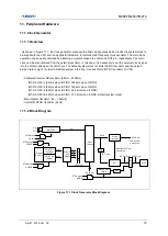
The clock generator register uses clock control for system operation. The clock generation consists of System
and clock control register and oscillator control register.
11.1.5 Register Description for Clock Generator
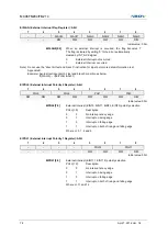
SCCR (System and Clock Control Register) : 8AH
7
6
5
4
3
2
1
0
WONS
–
–
–
–
–
SCLK1
SCLK0
R/W
–
–
–
–
–
R/W
R/W
Initial value : 00H
WONS
Control the Operation of WDT RC-Oscillation during STOP mode
0
WDTRC-Oscillator is disabled at STOP mode
1
WDTRC-Oscillator is enabled at STOP mode
NOTES)
1. When this bit is
“1”, the WDTRC oscillator (6kHz) is oscillated and
selected as the clock source of the WDT block in the STOP mode,
but the WDTRC stops and the BIT overflow clock is the clock
source for the WDT block at normal mode.
2. When this bit is
“0”, the WDTRC is always stopped and the BIT
overflow clock is selected as the clock source for the WDT block
SCLK [1:0]
System Clock Selection Bit
SCLK1 SCLK0 Description
0
0
HF-INT RC OSC (fHFIRC) for system clock
0
1
External Main OSC (fXIN) for system clock
1
0
LF-INT RC OSC (fLFIRC) for system clock
1
1
Not available
Summary of Contents for MC96FM204
Page 17: ...MC96FM204 FM214 April 7 2016 Ver 1 8 17 4 Package Diagram Figure 4 1 20 Pin SOP Package ...
Page 18: ...MC96FM204 FM214 18 April 7 2016 Ver 1 8 Figure 4 2 20 Pin TSSOP Package ...
Page 19: ...MC96FM204 FM214 April 7 2016 Ver 1 8 19 Figure 4 3 16 Pin SOP Package ...
Page 20: ...MC96FM204 FM214 20 April 7 2016 Ver 1 8 Figure 4 4 16 Pin TSSOP Package ...


