MC96F6432
48
June 22, 2018 Ver. 2.9
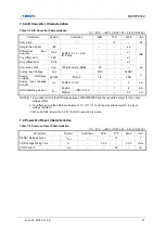
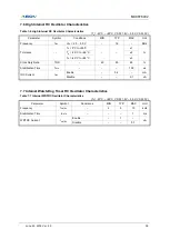
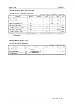
7.15 Internal Flash Rom Characteristics
Table 7-15 Internal Flash Rom Characteristics
(T
A
= -40°C ~ +85°C, VDD= 1.8V ~ 5.5V, VSS= 0V)
Parameter
Symbol
Condition
MIN
TYP
MAX
Unit
Sector Write Time
t
FSW
–
–
2.5
2.7
ms
Sector Erase Time
t
FSE
–
–
2.5
2.7
Code Write Protection Time
t
FHL
–
–
2.5
2.7
Page Buffer Reset Time
t
FBR
–
–
–
5
us
Flash Programming Frequency
f
PGM
–
0.4
–
–
MHz
Endurance of Write/Erase
NF
WE
–
–
–
100,000
Times
Flash Data Retention Time
t
RT
–
10
–
–
Years
NOTE) During a flash operation, SCLK[1:0] of SCCR must be set to
“00” or “01” (INT-RC OSC or Main X-TAL for
system clock).
7.16 Input/Output Capacitance
Table 7-16 Input/Output Capacitance
(T
A
= -40°C ~ +85°C, VDD= 0V)
Parameter
Symbol
Condition
MIN
TYP
MAX
Unit
Input Capacitance
C
IN
fx= 1MHz
Unmeasured pins are
connected to VSS
–
–
10
pF
Output Capacitance
C
OUT
I/O Capacitance
C
IO
Summary of Contents for MC96F6432 Series
Page 24: ...MC96F6432 24 June 22 2018 Ver 2 9 4 Package Diagram Figure 4 1 48 Pin LQFP 0707 Package...
Page 25: ...MC96F6432 June 22 2018 Ver 2 9 25 Figure 4 2 44 Pin MQFP Package...
Page 26: ...MC96F6432 26 June 22 2018 Ver 2 9 Figure 4 3 32 Pin LQFP Package...
Page 27: ...MC96F6432 June 22 2018 Ver 2 9 27 Figure 4 4 32 Pin SOP Package...
Page 28: ...MC96F6432 28 June 22 2018 Ver 2 9 Figure 4 5 28 Pin SOP Package...

