MC96F6432
36
June 22, 2018 Ver. 2.9
7. Electrical Characteristics
7.1 Absolute Maximum Ratings
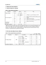
Table 7-1 Absolute Maximum Ratings
Parameter
Symbol
Rating
Unit
Note
Supply Voltage
VDD
-0.3 ~ +6.5
V
–
Normal Voltage Pin
V
I
-0.3 ~ VDD+0.3
V
Voltage on any pin with respect to VSS
V
O
-0.3 ~ VDD+0.3
V
I
OH
-10
mA
Maximum current output sourced by (I
OH
per
I/O pin)
∑
I
OH
-80
mA
Maximum current (
∑
I
OH
)
I
OL
60
mA
Maximum current sunk by (I
OL
per I/O pin)
∑
I
OL
120
mA
Maximum current (
∑
I
OL
)
Total Power
Dissipation
P
T
600
mW
–
Storage Temperature
T
STG
-65 ~ +150
°C
–
NOTE) Stresses beyond those listed under
“Absolute Maximum Ratings” may cause permanent damage to the
device. This is a stress rating only and functional operation of the device at any other conditions beyond those
indicated in the operational sections of this specification is not implied. Exposure to absolute maximum rating
conditions for extended periods may affect device reliability.
7.2 Recommended Operating Conditions
Table 7-2 Recommended Operating Conditions
(T
A
= -40°C ~ +85°C)
Parameter
Symbol
Conditions
MIN
TYP
MAX
Unit
Operating Voltage
VDD
f
X
= 32 ~ 38kHz
SX-tal
1.8
–
5.5
V
f
X
= 0.4 ~ 4.2MHz
X-tal
1.8
–
5.5
f
X
= 0.4 ~ 10.0MHz
2.7
–
5.5
f
X
= 0.4 ~ 12.0MHz
3.0
–
5.5
f
X
= 0.5 ~ 8.0MHz
Internal RC
1.8
–
5.5
f
X
= 0.5 ~ 16.0MHz
2.0
–
5.5
Operating Temperature
T
OPR
VDD= 1.8 ~ 5.5V
-40
–
85
°C
Summary of Contents for MC96F6432 Series
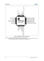
Page 24: ...MC96F6432 24 June 22 2018 Ver 2 9 4 Package Diagram Figure 4 1 48 Pin LQFP 0707 Package...
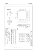
Page 25: ...MC96F6432 June 22 2018 Ver 2 9 25 Figure 4 2 44 Pin MQFP Package...
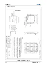
Page 26: ...MC96F6432 26 June 22 2018 Ver 2 9 Figure 4 3 32 Pin LQFP Package...
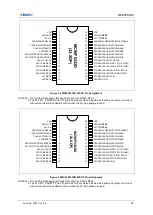
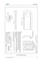
Page 27: ...MC96F6432 June 22 2018 Ver 2 9 27 Figure 4 4 32 Pin SOP Package...
Page 28: ...MC96F6432 28 June 22 2018 Ver 2 9 Figure 4 5 28 Pin SOP Package...

